0hmX/mq135-air-quality-sensor-module
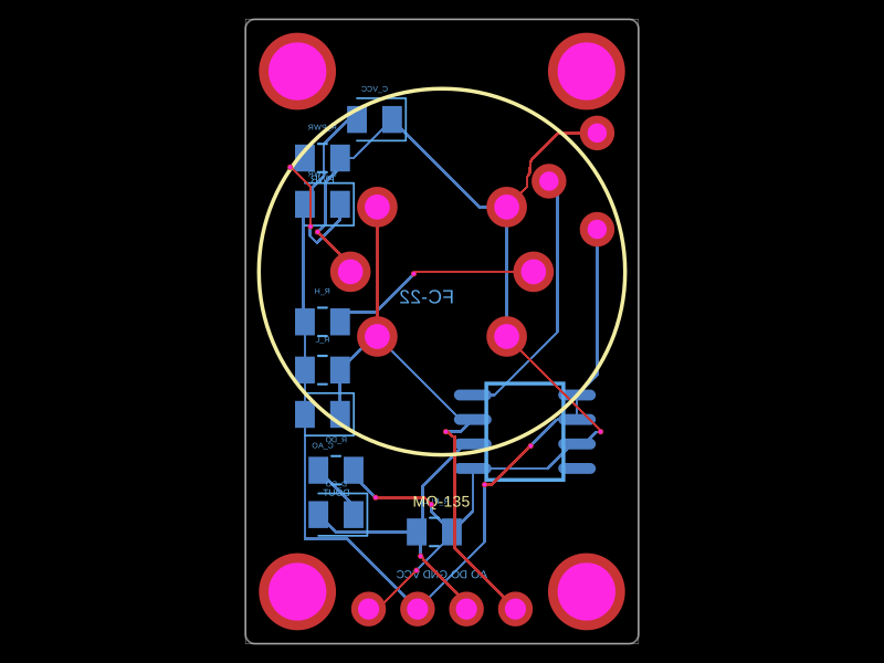
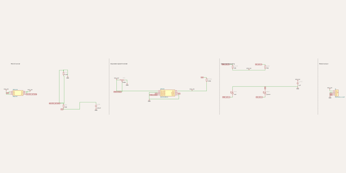
This code defines a detailed PCB and schematic design for a Winsen MQ-135 air quality sensor module featuring the sensor itself, a comparator IC, voltage regulators, LEDs, resistors, a potentiometer, pin headers, and associated physical component footprints.
- Version
- 1.0.1
- License
- unset
- Stars
- 0
index.circuit.tsx
PCB
Schematic
import mq135ModelUrl from "./models/mq135-sensor.glb"
import rightAngleHeaderModelUrl from "./models/right-angle-pin-header-1x4.glb"
import trimmerModelUrl from "./models/3362p-trimmer.glb"
import soic8ModelUrl from "./models/soic8.glb"
import { Fragment } from "react"

const SENSOR_SECTION = "sensor"
const COMPARATOR_SECTION = "comparator"
const INDICATOR_SECTION = "indicators"
const INTERFACE_SECTION = "interface"

// Winsen Configuration A, bottom view: diagonal sensing electrodes with the
// heater leads centered at left/right. The vertical 90°/270° positions are empty.
const sensorPinAngles = [225, 180, 135, 45, 0, 315]
const sensorPinPositions = sensorPinAngles.map((angleDegrees, pinIndex) => {
  const pin = pinIndex + 1
  const angle = (angleDegrees * Math.PI) / 180
  return { pin, x: 4.75 * Math.cos(angle), y: 4.75 * Math.sin(angle) }
})

const headerPinX = [-3.81, -1.27, 1.27, 3.81]

/** Reproduction of the Robocraze/Amazon blue FC-22 MQ-135 breakout. */
export default function MQ135AirQualitySensorModule() {
  return (
    <board
      width="20.4mm"
      height="32.4mm"
      layers={2}
      borderRadius="0.5mm"
      thickness="1.6mm"
      solderMaskColor="blue"
      silkscreenColor="white"
      doubleSidedAssembly
      minBoardEdgeClearance="0.2mm"
    >
      <net name="VCC_5V" />
      <net name="GND" />
      <net name="AO" />
      <net name="THRESHOLD" />
      <net name="DO" />
      <net name="PWR_LED_A" />
      <net name="DO_LED_A" />
      <net name="HEATER_RETURN" />

      <schematicsection name={SENSOR_SECTION} displayName="MQ-135 sensor" />
      <schematicsection
        name={COMPARATOR_SECTION}
        displayName="Adjustable digital threshold"
      />
      <schematicsection
        name={INDICATOR_SECTION}
        displayName="Status and decoupling"
      />
      <schematicsection name={INTERFACE_SECTION} displayName="Module output" />

      <chip
        name="MQ1"
        displayName="MQ-135"
        manufacturerPartNumber="MQ135"
        datasheetUrl="https://www.winsen-sensor.com/d/files/mq135-%28ver1_6%29---manual.pdf"
        pinLabels={{
          pin1: "B1",
          pin2: "H1",
          pin3: "B2",
          pin4: "A2",
          pin5: "H2",
          pin6: "A1",
        }}
        pinAttributes={{
          B1: { mustBeConnected: true },
          H1: {
            mustBeConnected: true,
            requiresPower: true,
            requiresVoltage: "5V",
          },
          B2: { mustBeConnected: true },
          A2: { mustBeConnected: true },
          H2: { mustBeConnected: true, requiresGround: true },
          A1: { mustBeConnected: true },
        }}
        internallyConnectedPins={[
          ["pin1", "pin3"],
          ["pin4", "pin6"],
        ]}
        schPinArrangement={{
          leftSide: {
            pins: ["B1", "B2", "H1"],
            direction: "top-to-bottom",
          },
          rightSide: {
            pins: ["A1", "A2", "H2"],
            direction: "top-to-bottom",
          },
        }}
        schSectionName={SENSOR_SECTION}
        schX={-16}
        schY={3}
        schWidth={1.58}
        schHeight={0.8}
        pcbX={0}
        pcbY={3.1}
        footprint={
          <footprint>
            {sensorPinPositions.map(({ pin, x, y }) => (
              <Fragment key={pin}>
                <platedhole
                  portHints={[`pin${pin}`]}
                  pcbX={x}
                  pcbY={y}
                  shape="circle"
                  holeDiameter="1.3mm"
                  outerDiameter="2.1mm"
                />
              </Fragment>
            ))}
            <silkscreencircle radius="9.5mm" strokeWidth="0.2mm" />
          </footprint>
        }
        cadModel={{ glbUrl: mq135ModelUrl, modelBoardNormalDirection: "z+" }}
      />

      <resistor
        name="R_H"
        displayName="5R1"
        resistance="5.1ohm"
        footprint="0805"
        supplierPartNumbers={{ jlcpcb: ["C313941"] }}
        manufacturerPartNumber="CRCW08055R10FKEAHP"
        layer="bottom"
        schSectionName={SENSOR_SECTION}
        schX={-9}
        schY={6}
        schRotation={90}
        pcbX={-6.2}
        pcbY={0.5}
      />
      <resistor
        name="R_L"
        displayName="202"
        resistance="2kohm"
        footprint="0805"
        supplierPartNumbers={{ jlcpcb: ["C17604"] }}
        manufacturerPartNumber="0805W8F2001T5E"
        layer="bottom"
        schSectionName={SENSOR_SECTION}
        schX={-9}
        schY={1}
        schRotation={90}
        pcbX={-6.2}
        pcbY={-2}
      />
      <capacitor
        name="C_AO"
        capacitance="100nF"
        footprint="0805"
        supplierPartNumbers={{ jlcpcb: ["C49678"] }}
        manufacturerPartNumber="CC0805KRX7R9BB104"
        layer="bottom"
        schSectionName={SENSOR_SECTION}
        schX={-4}
        schY={1}
        schOrientation="vertical"
        pcbX={-6.2}
        pcbY={-4.3}
      />

      <potentiometer
        name="RV1"
        displayName="103"
        maxResistance="10kohm"
        pinVariant="three_pin"
        supplierPartNumbers={{ jlcpcb: ["C118956"] }}
        manufacturerPartNumber="3362P-1-103"
        layer="bottom"
        schSectionName={COMPARATOR_SECTION}
        schX={0}
        schY={5}
        pcbX={6.8}
        pcbY={7.8}
        pcbRotation={90}
        footprint={
          <footprint>
            <platedhole
              portHints={["pin1"]}
              pcbX={-2.5}
              pcbY={-1.25}
              shape="circle"
              holeDiameter="1mm"
              outerDiameter="1.8mm"
            />
            <platedhole
              portHints={["pin2"]}
              pcbX={0}
              pcbY={1.25}
              shape="circle"
              holeDiameter="1mm"
              outerDiameter="1.8mm"
            />
            <platedhole
              portHints={["pin3"]}
              pcbX={2.5}
              pcbY={-1.25}
              shape="circle"
              holeDiameter="1mm"
              outerDiameter="1.8mm"
            />
          </footprint>
        }
        cadModel={{ glbUrl: trimmerModelUrl, modelBoardNormalDirection: "z+" }}
      />

      <chip
        name="U1"
        displayName="LM393"
        manufacturerPartNumber="LM393DR2G"
        supplierPartNumbers={{ jlcpcb: ["C7955"] }}
        footprint={
          <footprint>
            {[
              { pin: 1, x: -2.7051, y: -1.905 },
              { pin: 2, x: -2.7051, y: -0.635 },
              { pin: 3, x: -2.7051, y: 0.635 },
              { pin: 4, x: -2.7051, y: 1.905 },
              { pin: 5, x: 2.7051, y: 1.905 },
              { pin: 6, x: 2.7051, y: 0.635 },
              { pin: 7, x: 2.7051, y: -0.635 },
              { pin: 8, x: 2.7051, y: -1.905 },
            ].map(({ pin, x, y }) => (
              <Fragment key={pin}>
                <smtpad
                  portHints={[`pin${pin}`]}
                  shape="pill"
                  pcbX={x}
                  pcbY={y}
                  width="1.9502mm"
                  height="0.5684mm"
                  radius="0.2842mm"
                />
              </Fragment>
            ))}
            <silkscreenrect width="4mm" height="5mm" strokeWidth="0.2mm" />
          </footprint>
        }
        cadModel={{ glbUrl: soic8ModelUrl, modelBoardNormalDirection: "z+" }}
        layer="bottom"
        pinLabels={{
          pin1: "OUTA",
          pin2: "INA_NEG",
          pin3: "INA_POS",
          pin4: "GND",
          pin5: "INB_POS",
          pin6: "INB_NEG",
          pin7: "OUTB",
          pin8: "VCC",
        }}
        pinAttributes={{
          OUTA: { doNotConnect: true },
          INA_NEG: { mustBeConnected: true },
          INA_POS: { mustBeConnected: true },
          GND: { mustBeConnected: true, requiresGround: true },
          INB_POS: { mustBeConnected: true },
          INB_NEG: { mustBeConnected: true },
          OUTB: { mustBeConnected: true },
          VCC: {
            mustBeConnected: true,
            requiresPower: true,
            requiresVoltage: "5V",
            shouldHaveDecouplingCapacitor: true,
            recommendedDecouplingCapacitorCapacitance: "1uF",
          },
        }}
        noConnect={["OUTA"]}
        schPinArrangement={{
          leftSide: {
            pins: ["INA_NEG", "INA_POS", "INB_NEG", "INB_POS"],
            direction: "top-to-bottom",
          },
          rightSide: {
            pins: ["VCC", "OUTA", "OUTB", "GND"],
            direction: "top-to-bottom",
          },
        }}
        schSectionName={COMPARATOR_SECTION}
        schX={7}
        schY={3}
        schWidth={2.245}
        schHeight={1}
        pcbX={4.3}
        pcbY={-5.2}
      />
      <resistor
        name="R_PULL"
        resistance="10kohm"
        footprint="0805"
        supplierPartNumbers={{ jlcpcb: ["C17414"] }}
        manufacturerPartNumber="0805W8F1002T5E"
        layer="bottom"
        schSectionName={COMPARATOR_SECTION}
        schX={13}
        schY={5}
        schRotation={90}
        pcbX={-0.4}
        pcbY={-10.4}
      />

      <resistor
        name="R_PWR"
        resistance="1kohm"
        footprint="0805"
        supplierPartNumbers={{ jlcpcb: ["C17513"] }}
        manufacturerPartNumber="0805W8F1001T5E"
        layer="bottom"
        schSectionName={INDICATOR_SECTION}
        schX={17}
        schY={7}
        schRotation={90}
        pcbX={-6.2}
        pcbY={9}
      />
      <led
        name="D_PWR"
        displayName="PWR"
        color="red"
        footprint="0805"
        supplierPartNumbers={{ jlcpcb: ["C84256"] }}
        manufacturerPartNumber="NCD0805R1"
        layer="bottom"
        schSectionName={INDICATOR_SECTION}
        schX={17}
        schY={3}
        schRotation={90}
        pcbX={-6.2}
        pcbY={6.6}
      />
      <resistor
        name="R_DO"
        resistance="1kohm"
        footprint="0805"
        supplierPartNumbers={{ jlcpcb: ["C17513"] }}
        manufacturerPartNumber="0805W8F1001T5E"
        layer="bottom"
        schSectionName={INDICATOR_SECTION}
        schX={22}
        schY={7}
        schRotation={90}
        pcbX={-5.5}
        pcbY={-7.2}
      />
      <led
        name="D_DO"
        displayName="DOUT"
        color="green"
        footprint="0805"
        supplierPartNumbers={{ jlcpcb: ["C2297"] }}
        manufacturerPartNumber="KT-0805G"
        layer="bottom"
        schSectionName={INDICATOR_SECTION}
        schX={22}
        schY={3}
        schRotation={90}
        pcbX={-5.5}
        pcbY={-9.5}
      />
      <capacitor
        name="C_VCC"
        capacitance="1uF"
        footprint="0805"
        supplierPartNumbers={{ jlcpcb: ["C28323"] }}
        manufacturerPartNumber="CL21B105KBFNNNE"
        layer="bottom"
        schSectionName={INDICATOR_SECTION}
        schX={27}
        schY={4.5}
        schOrientation="vertical"
        pcbX={-3.5}
        pcbY={11}
      />

      <pinheader
        name="J1"
        pinCount={4}
        pitch="2.54mm"
        gender="male"
        rightAngle
        manufacturerPartNumber="PZ254R-11-04P"
        supplierPartNumbers={{ jlcpcb: ["C492412"] }}
        pinLabels={{ pin1: "VCC", pin2: "GND", pin3: "DO", pin4: "AO" }}
        pcbPinLabels={{ pin1: "VCC", pin2: "GND", pin3: "DO", pin4: "AO" }}
        pinAttributes={{
          VCC: {
            providesPower: true,
            providesVoltage: "5V",
            includeInBoardPinout: true,
          },
          GND: { providesGround: true, includeInBoardPinout: true },
          DO: { includeInBoardPinout: true },
          AO: { includeInBoardPinout: true },
        }}
        schFacingDirection="left"
        schSectionName={INTERFACE_SECTION}
        schX={33}
        schY={3}
        schWidth={0.485}
        pcbX={0}
        pcbY={-14.4}
        footprint={
          <footprint insertionDirection="from_bottom">
            {headerPinX.map((x, pinIndex) => (
              <Fragment key={pinIndex}>
                <platedhole
                  portHints={[`pin${pinIndex + 1}`]}
                  pcbX={x}
                  pcbY={0}
                  shape="circle"
                  holeDiameter="1.1mm"
                  outerDiameter="1.8mm"
                />
              </Fragment>
            ))}
          </footprint>
        }
        cadModel={{
          glbUrl: rightAngleHeaderModelUrl,
          modelBoardNormalDirection: "z+",
        }}
      />

      <trace name="MQ_A1_VCC" from=".MQ1 > .A1" to="net.VCC_5V" />
      <trace name="MQ_A2_VCC" from=".MQ1 > .A2" to="net.VCC_5V" />
      <trace name="MQ_B1_AO" from=".MQ1 > .B1" to="net.AO" />
      <trace name="MQ_B2_AO" from=".MQ1 > .B2" to="net.AO" />
      <trace name="MQ_H1_VCC" from=".MQ1 > .H1" to="net.VCC_5V" />
      <trace name="MQ_H2_RETURN" from=".MQ1 > .H2" to="net.HEATER_RETURN" />
      <trace name="RH_RETURN" from=".R_H > .pin1" to="net.HEATER_RETURN" />
      <trace name="RH_GND" from=".R_H > .pin2" to="net.GND" />
      <trace name="RL_AO" from=".R_L > .pin1" to="net.AO" />
      <trace name="RL_GND" from=".R_L > .pin2" to="net.GND" />
      <trace name="CAO_AO" from=".C_AO > .pin1" to="net.AO" />
      <trace name="CAO_GND" from=".C_AO > .pin2" to="net.GND" />

      <trace name="RV1_VCC" from=".RV1 > .pin1" to="net.VCC_5V" />
      <trace name="RV1_REF" from=".RV1 > .pin2" to="net.THRESHOLD" />
      <trace name="RV1_GND" from=".RV1 > .pin3" to="net.GND" />
      <trace name="U1_VCC" from=".U1 > .VCC" to="net.VCC_5V" />
      <trace name="U1_GND" from=".U1 > .GND" to="net.GND" />
      <trace name="U1_INA_NEG" from=".U1 > .INA_NEG" to="net.VCC_5V" />
      <trace name="U1_INA_POS" from=".U1 > .INA_POS" to="net.GND" />
      <trace name="U1_INB_NEG" from=".U1 > .INB_NEG" to="net.AO" />
      <trace name="U1_INB_POS" from=".U1 > .INB_POS" to="net.THRESHOLD" />
      <trace name="U1_OUTB" from=".U1 > .OUTB" to="net.DO" />
      <trace name="RPULL_VCC" from=".R_PULL > .pin1" to="net.VCC_5V" />
      <trace name="RPULL_DO" from=".R_PULL > .pin2" to="net.DO" />

      <trace name="RPWR_VCC" from=".R_PWR > .pin1" to="net.VCC_5V" />
      <trace name="RPWR_LED" from=".R_PWR > .pin2" to="net.PWR_LED_A" />
      <trace name="DPWR_A" from=".D_PWR > .anode" to="net.PWR_LED_A" />
      <trace name="DPWR_K" from=".D_PWR > .cathode" to="net.GND" />
      <trace name="RDO_VCC" from=".R_DO > .pin1" to="net.VCC_5V" />
      <trace name="RDO_LED" from=".R_DO > .pin2" to="net.DO_LED_A" />
      <trace name="DDO_A" from=".D_DO > .anode" to="net.DO_LED_A" />
      <trace name="DDO_K" from=".D_DO > .cathode" to="net.DO" />
      <trace name="CVCC_VCC" from=".C_VCC > .pin1" to="net.VCC_5V" />
      <trace name="CVCC_GND" from=".C_VCC > .pin2" to="net.GND" />

      <trace name="J1_VCC" from=".J1 > .VCC" to="net.VCC_5V" />
      <trace name="J1_GND" from=".J1 > .GND" to="net.GND" />
      <trace name="J1_DO" from=".J1 > .DO" to="net.DO" />
      <trace name="J1_AO" from=".J1 > .AO" to="net.AO" />

      <platedhole
        name="H1"
        shape="circle"
        holeDiameter="3mm"
        outerDiameter="4mm"
        pcbX={-7.5}
        pcbY={13.5}
      />
      <platedhole
        name="H2"
        shape="circle"
        holeDiameter="3mm"
        outerDiameter="4mm"
        pcbX={7.5}
        pcbY={13.5}
      />
      <platedhole
        name="H3"
        shape="circle"
        holeDiameter="3mm"
        outerDiameter="4mm"
        pcbX={-7.5}
        pcbY={-13.5}
      />
      <platedhole
        name="H4"
        shape="circle"
        holeDiameter="3mm"
        outerDiameter="4mm"
        pcbX={7.5}
        pcbY={-13.5}
      />

      <silkscreentext
        text="MQ-135"
        pcbX={0}
        pcbY={-8.8}
        fontSize="0.8mm"
        anchorAlignment="center"
      />
      <silkscreentext
        text="FC-22"
        layer="bottom"
        pcbX={-0.8}
        pcbY={1.8}
        fontSize="1mm"
        anchorAlignment="center"
      />
      <silkscreentext
        text="AO  DO  GND  VCC"
        layer="bottom"
        pcbX={0}
        pcbY={-12.6}
        fontSize="0.58mm"
        anchorAlignment="center"
      />
      <silkscreentext
        text="PWR"
        layer="bottom"
        pcbX={-6.2}
        pcbY={7.9}
        fontSize="0.55mm"
        anchorAlignment="center"
      />
      <silkscreentext
        text="DOUT"
        layer="bottom"
        pcbX={-5.5}
        pcbY={-8.35}
        fontSize="0.5mm"
        anchorAlignment="center"
      />
    </board>
  )
}
Related Packages
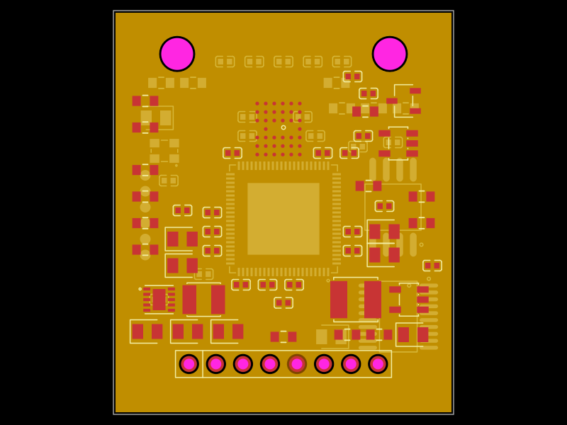 More from this author0hmX/arducam-mini-2mp-plus-b0067-cloneThis code defines React components representing various hardware electronic components such as sensors, chips, capacitors, inductors, and memory devices, including their physical pin layouts, footprints, and 3D CAD models for PCB design integration.
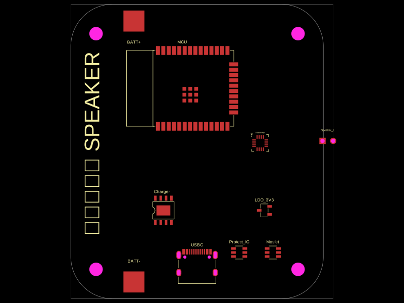 Similar packagemohan-bee/speakerThis code defines configurable 3D models and PCB footprints for various electronic components, including a battery charger IC, a dual Hall sensor, a dual power switch, and a voltage regulator, with detailed pinouts, footprints, and CAD models for schematic and physical design.
 Discover something newShiboSoftwareDev/mspm0g3507-usb-c-dev-boardThe circuit assembles a USB-C port with integrated ESD protection, power regulation, UART interface, and microcontroller (MSPM0G3507) with supporting components for USB data lines, CC termination, I2C, SPI, reset circuitry, and indicator LEDs.