ShiboSoftwareDev/am625sip-linux-board
This code defines the physical footprint and pin layout for an AM625 System-in-Package (SIP) component, detailing pad positions, pin labels, and package outline for hardware integration.
- Version
- 1.0.24
- License
- unset
- Stars
- 0
subcircuits/cache/__snapshots__/usb0-data-esd.circuit-pcb.snap.svg
<svg xmlns="http://www.w3.org/2000/svg" width="800" height="600"><style></style><rect class="boundary" x="0" y="0" fill="#000" width="800" height="600" data-type="pcb_background" data-pcb-layer="global"/><rect class="pcb-boundary" fill="none" stroke="#fff" stroke-width="0.3" x="142.8571428571429" y="85.71428571428572" width="514.2857142857142" height="428.5714285714285" data-type="pcb_boundary" data-pcb-layer="global"/><path class="pcb-board" d="M 142.8571428571429 514.2857142857142 L 657.1428571428571 514.2857142857142 L 657.1428571428571 85.71428571428572 L 142.8571428571429 85.71428571428572 Z" fill="none" stroke="rgba(255, 255, 255, 0.5)" stroke-width="8.571428571428571" data-type="pcb_board" data-pcb-layer="board"/><path class="pcb-trace" stroke="rgb(255, 140, 0)" fill="none" d="M 359.7142857142857 309 L 360.41175014198694 309.6974644277012" stroke-width="25.71428571428571" stroke-linecap="round" stroke-linejoin="round" shape-rendering="crispEdges" data-type="pcb_trace" data-pcb-layer="inner1"/><path class="pcb-trace" stroke="rgb(255, 140, 0)" fill="none" d="M 360.41175014198694 309.6974644277012 L 363.64658002567376 312.9322943113881" stroke-width="25.71428571428571" stroke-linecap="round" stroke-linejoin="round" shape-rendering="crispEdges" data-type="pcb_trace" data-pcb-layer="inner1"/><path class="pcb-trace" stroke="rgb(255, 140, 0)" fill="none" d="M 363.64658002567376 312.9322943113881 L 363.64658002567376 316.3932683036226" stroke-width="25.71428571428571" stroke-linecap="round" stroke-linejoin="round" shape-rendering="crispEdges" data-type="pcb_trace" data-pcb-layer="inner1"/><path class="pcb-trace" stroke="rgb(255, 140, 0)" fill="none" d="M 363.64658002567376 316.3932683036226 L 363.64658002567376 318.91047361645377" stroke-width="25.71428571428571" stroke-linecap="round" stroke-linejoin="round" shape-rendering="crispEdges" data-type="pcb_trace" data-pcb-layer="inner1"/><path class="pcb-trace" stroke="rgb(255, 140, 0)" fill="none" d="M 363.64658002567376 318.91047361645377 L 367.54875514243827 322.8126487332183" stroke-width="25.71428571428571" stroke-linecap="round" stroke-linejoin="round" shape-rendering="crispEdges" data-type="pcb_trace" data-pcb-layer="inner1"/><path class="pcb-trace" stroke="rgb(255, 140, 0)" fill="none" d="M 367.54875514243827 322.8126487332183 L 373.23086320554444 328.49475679632445" stroke-width="25.71428571428571" stroke-linecap="round" stroke-linejoin="round" shape-rendering="crispEdges" data-type="pcb_trace" data-pcb-layer="inner1"/><path class="pcb-trace" stroke="rgb(255, 140, 0)" fill="none" d="M 373.23086320554444 328.49475679632445 L 378.9129712686506 334.1768648594306" stroke-width="25.71428571428571" stroke-linecap="round" stroke-linejoin="round" shape-rendering="crispEdges" data-type="pcb_trace" data-pcb-layer="inner1"/><path class="pcb-trace" stroke="rgb(255, 140, 0)" fill="none" d="M 378.9129712686506 334.1768648594306 L 400 355.26389359078" stroke-width="25.71428571428571" stroke-linecap="round" stroke-linejoin="round" shape-rendering="crispEdges" data-type="pcb_trace" data-pcb-layer="inner1"/><path class="pcb-trace" stroke="rgb(255, 140, 0)" fill="none" d="M 400 355.26389359078 L 400 428.57142857142856" stroke-width="25.71428571428571" stroke-linecap="round" stroke-linejoin="round" shape-rendering="crispEdges" data-type="pcb_trace" data-pcb-layer="inner1"/><rect class="pcb-pad" fill="rgb(200, 52, 52)" x="215.71428571428572" y="252.85714285714286" width="25.71428571428571" height="25.71428571428571" data-type="pcb_smtpad" data-pcb-layer="top"/><rect class="pcb-pad" fill="rgb(200, 52, 52)" x="215.71428571428572" y="321.42857142857144" width="25.71428571428571" height="25.71428571428571" data-type="pcb_smtpad" data-pcb-layer="top"/><rect class="pcb-pad" fill="rgb(200, 52, 52)" x="558.5714285714286" y="252.85714285714286" width="25.71428571428571" height="25.71428571428571" data-type="pcb_smtpad" data-pcb-layer="top"/><rect class="pcb-pad" fill="rgb(200, 52, 52)" x="558.5714285714286" y="321.42857142857144" width="25.71428571428571" height="25.71428571428571" data-type="pcb_smtpad" data-pcb-layer="top"/><rect class="pcb-pad" fill="rgb(200, 52, 52)" x="404.28461714285714" y="262.2875314285714" width="17.142822857142857" height="17.142822857142857" data-type="pcb_smtpad" data-pcb-layer="top"/><rect class="pcb-pad" fill="rgb(200, 52, 52)" x="404.28461714285714" y="320.56964571428574" width="17.142822857142857" height="17.142822857142857" data-type="pcb_smtpad" data-pcb-layer="top"/><rect class="pcb-pad" fill="rgb(200, 52, 52)" x="378.57256" y="291.41770285714284" width="17.142822857142857" height="17.142822857142857" data-type="pcb_smtpad" data-pcb-layer="top"/><path class="pcb-trace" stroke="rgb(200, 52, 52)" fill="none" d="M 412.85602857142857 329.14105714285716 L 418.00068571428574 334.2857142857143" stroke-width="12.857142857142856" stroke-linecap="round" stroke-linejoin="round" shape-rendering="crispEdges" data-type="pcb_trace" data-pcb-layer="top"/><path class="pcb-trace" stroke="rgb(200, 52, 52)" fill="none" d="M 418.00068571428574 334.2857142857143 L 571.4285714285714 334.2857142857143" stroke-width="12.857142857142856" stroke-linecap="round" stroke-linejoin="round" shape-rendering="crispEdges" data-type="pcb_trace" data-pcb-layer="top"/><path class="pcb-trace" stroke="rgb(200, 52, 52)" fill="none" d="M 228.57142857142858 334.2857142857143 L 407.7113714285714 334.2857142857143" stroke-width="12.857142857142856" stroke-linecap="round" stroke-linejoin="round" shape-rendering="crispEdges" data-type="pcb_trace" data-pcb-layer="top"/><path class="pcb-trace" stroke="rgb(200, 52, 52)" fill="none" d="M 407.7113714285714 334.2857142857143 L 412.85602857142857 329.14105714285716" stroke-width="12.857142857142856" stroke-linecap="round" stroke-linejoin="round" shape-rendering="crispEdges" data-type="pcb_trace" data-pcb-layer="top"/><path class="pcb-trace" stroke="rgb(200, 52, 52)" fill="none" d="M 412.85602857142857 270.85894285714284 L 418.00068571428574 265.7142857142857" stroke-width="12.857142857142856" stroke-linecap="round" stroke-linejoin="round" shape-rendering="crispEdges" data-type="pcb_trace" data-pcb-layer="top"/><path class="pcb-trace" stroke="rgb(200, 52, 52)" fill="none" d="M 418.00068571428574 265.7142857142857 L 571.4285714285714 265.7142857142857" stroke-width="12.857142857142856" stroke-linecap="round" stroke-linejoin="round" shape-rendering="crispEdges" data-type="pcb_trace" data-pcb-layer="top"/><path class="pcb-trace" stroke="rgb(200, 52, 52)" fill="none" d="M 228.57142857142858 265.7142857142857 L 407.7113714285714 265.7142857142857" stroke-width="12.857142857142856" stroke-linecap="round" stroke-linejoin="round" shape-rendering="crispEdges" data-type="pcb_trace" data-pcb-layer="top"/><path class="pcb-trace" stroke="rgb(200, 52, 52)" fill="none" d="M 407.7113714285714 265.7142857142857 L 412.85602857142857 270.85894285714284" stroke-width="12.857142857142856" stroke-linecap="round" stroke-linejoin="round" shape-rendering="crispEdges" data-type="pcb_trace" data-pcb-layer="top"/><path class="pcb-trace" stroke="rgb(200, 52, 52)" fill="none" d="M 387.14397142857143 299.98911428571427 L 381.46074907975094 305.68210806310617" stroke-width="24.243603638841886" stroke-linecap="round" stroke-linejoin="round" shape-rendering="crispEdges" data-type="pcb_trace" data-pcb-layer="top"/><path class="pcb-trace" stroke="rgb(200, 52, 52)" fill="none" d="M 381.46074907975094 305.68210806310617 L 378.5714457142857 308.5714114285714" stroke-width="24.24361258193092" stroke-linecap="round" stroke-linejoin="round" shape-rendering="crispEdges" data-type="pcb_trace" data-pcb-layer="top"/><path class="pcb-trace" stroke="rgb(200, 52, 52)" fill="none" d="M 378.5714457142857 308.5714114285714 L 378.14285714285717 309" stroke-width="24.26070099061959" stroke-linecap="round" stroke-linejoin="round" shape-rendering="crispEdges" data-type="pcb_trace" data-pcb-layer="top"/><path class="pcb-trace" stroke="rgb(200, 52, 52)" fill="none" d="M 378.14285714285717 309 L 374.7993506327864 309" stroke-width="24.35496549995638" stroke-linecap="round" stroke-linejoin="round" shape-rendering="crispEdges" data-type="pcb_trace" data-pcb-layer="top"/><path class="pcb-trace" stroke="rgb(200, 52, 52)" fill="none" d="M 374.7993506327864 309 L 366.7636363470721 309" stroke-width="24.581518869011266" stroke-linecap="round" stroke-linejoin="round" shape-rendering="crispEdges" data-type="pcb_trace" data-pcb-layer="top"/><path class="pcb-trace" stroke="rgb(200, 52, 52)" fill="none" d="M 366.7636363470721 309 L 359.7142857142857 309" stroke-width="24.780263383652137" stroke-linecap="round" stroke-linejoin="round" shape-rendering="crispEdges" data-type="pcb_trace" data-pcb-layer="top"/><path class="pcb-silkscreen pcb-silkscreen-top" d="M 438.5746171428569 245.1425314285773 L 361.4319142857117 245.1425314285773 L 361.4319142857117 356.5708800000006 L 438.5746171428569 356.5708800000006 L 438.5746171428569 245.1425314285773 Z" fill="none" stroke="#f2eda1" stroke-width="8.571428571428571" stroke-linecap="round" stroke-linejoin="round" data-pcb-component-id="pcb_component_5" data-pcb-silkscreen-path-id="pcb_silkscreen_path_0" data-type="pcb_silkscreen_path" data-pcb-layer="top"/><text x="0" y="0" dx="0" dy="0" fill="#f2eda1" font-family="Arial, sans-serif" font-size="85.71428571428571" text-anchor="middle" dominant-baseline="central" transform="matrix(1,0,0,1,399.7714,159.84625714285716)" class="pcb-silkscreen-text pcb-silkscreen-top" data-pcb-silkscreen-text-id="pcb_silkscreen_text_0" stroke="none" data-type="pcb_silkscreen_text" data-pcb-layer="top">U5</text><g data-type="pcb_plated_hole" data-pcb-layer="through"><circle class="pcb-hole-outer" fill="rgb(200, 52, 52)" cx="400" cy="428.57142857142856" r="34.285714285714285" data-type="pcb_plated_hole" data-pcb-layer="top"/><circle class="pcb-hole-inner" fill="#FF26E2" cx="400" cy="428.57142857142856" r="12.857142857142856" data-type="pcb_plated_hole_drill" data-pcb-layer="drill"/></g><g data-type="pcb_via" data-pcb-layer="through"><circle class="pcb-hole-outer" fill="rgb(200, 52, 52)" cx="359.7142857142857" cy="309" r="10.285714285714285" data-type="pcb_via" data-pcb-layer="top"/><circle class="pcb-hole-inner" fill="#FF26E2" cx="359.7142857142857" cy="309" r="4.285714285714286" data-type="pcb_via" data-pcb-layer="drill"/></g></svg>Related Packages
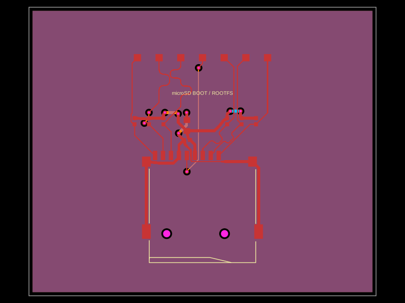 More from this authorShiboSoftwareDev/t113-s3-linux-computer-p9The code defines a PCB subcircuit for a buck converter module featuring a TMI3112H IC, FTC252010S power switch, and associated passive components like capacitors and resistors for voltage regulation and feedback control.
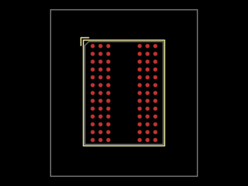 Similar package0hmX/mt41k512m8da-107-it-p-footprintsThis code defines the mechanical and physical layout of a Micron digital ball grid array (FBGA) package with 78 balls, including pin positions, footprint geometry, PCB pads, and silkscreen outlines for surface-mount integration.
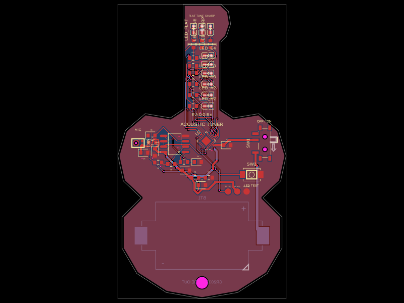 Discover something newgokul/acoustic-guitar-tunerThis code defines a miniature circuit board featuring a microcontroller (ATTINY1616-MNR), audio and power components, tactile switch, various LEDs, and passive components arranged with specific footprints, connections, and mechanical markings for a mini acoustic guitar tuner.