imrishabh18/pedometer
This code defines and assembles a simple radio receiver hardware circuit using specific imported capacitors, inductors, RF connectors, and oscillator components with precise footprints and schematic attributes.
- Version
- 1.1.3
- License
- unset
- Stars
- 0
manufacturing.ts
import type { AnyCircuitElement, PcbSolderPaste } from "circuit-json"

/** TI YFP0020 / YZF0009, 0.10 mm stencil. Rounded-square apertures are
 * represented as the union of two rectangles and four circles because the
 * current Circuit JSON solder-paste schema has no rounded-rectangle primitive.
 * No copper, drill positions, or routing are added or moved here. */
export function prepareManufacturingCircuit(input: AnyCircuitElement[]) {
  const c = structuredClone(input)
  const sourceIds = new Set(c.filter(e => e.type === "source_component" &&
    "manufacturer_part_number" in e &&
    ["BQ25150YFPR", "BQ27427YZFR"].includes(e.manufacturer_part_number ?? ""))
    .map(e => e.type === "source_component" ? e.source_component_id : ""))
  const componentIds = new Set(c.filter(e => e.type === "pcb_component" &&
    sourceIds.has(e.source_component_id)).map(e => e.type === "pcb_component" ? e.pcb_component_id : ""))
  const pads = c.filter(e => e.type === "pcb_smtpad" && componentIds.has(e.pcb_component_id ?? ""))
  if (componentIds.size !== 2 || pads.length !== 29) throw new Error("Expected both BGA components and all 29 lands")
  const ids = new Set(pads.map(p => p.type === "pcb_smtpad" ? p.pcb_smtpad_id : ""))
  const result = c.filter(e => e.type !== "pcb_solder_paste" || !ids.has(e.pcb_smtpad_id ?? ""))
  for (const pad of pads) {
    if (pad.type !== "pcb_smtpad" || pad.shape !== "circle") throw new Error("BGA copper must be circular")
    const viaInPad = c.some(e => e.type === "pcb_via" &&
      Math.hypot(e.x - pad.x, e.y - pad.y) < pad.radius + e.hole_diameter / 2)
    // Capped via annuli are larger than the TI land. Retain the TI solderable
    // opening rather than exposing the complete annulus; assembler qualification
    // of these SMD openings remains required. Other lands use +0.025 mm
    // radial NSMD expansion to retain >=0.10 mm mask bridges at 0.4 mm pitch.
    pad.soldermask_margin = viaInPad ? 0 : 0.025
    const common = {
      type: "pcb_solder_paste" as const, layer: pad.layer,
      pcb_smtpad_id: pad.pcb_smtpad_id, pcb_component_id: pad.pcb_component_id,
      subcircuit_id: pad.subcircuit_id,
    }
    const width = 0.25, radius = 0.05, offset = width / 2 - radius
    const shapes: PcbSolderPaste[] = [
      { ...common, pcb_solder_paste_id: `${pad.pcb_smtpad_id}_paste_h`, shape: "rect", x: pad.x, y: pad.y, width, height: width - 2 * radius },
      { ...common, pcb_solder_paste_id: `${pad.pcb_smtpad_id}_paste_v`, shape: "rect", x: pad.x, y: pad.y, width: width - 2 * radius, height: width },
    ]
    for (const dx of [-offset, offset]) for (const dy of [-offset, offset]) {
      shapes.push({ ...common, pcb_solder_paste_id: `${pad.pcb_smtpad_id}_paste_${dx}_${dy}`,
        shape: "circle", x: pad.x + dx, y: pad.y + dy, radius })
    }
    result.push(...shapes)
  }
  // TI RGE0024B exposed-pad stencil: four 1.08 mm windows at +/-0.64 mm,
  // R0.05 corners (~78% coverage). TI illustrates a 0.125 mm stencil;
  // the common stencil thickness with the BGAs needs assembler approval.
  const mcu = c.find(e=>e.type==="source_component" && e.manufacturer_part_number==="CC2340R52E0RGER")
  const mcuPcb = mcu?.type==="source_component" ? c.find(e=>e.type==="pcb_component" && e.source_component_id===mcu.source_component_id) : undefined
  const ep = mcuPcb?.type==="pcb_component" ? c.find(e=>e.type==="pcb_smtpad" && e.pcb_component_id===mcuPcb.pcb_component_id && e.port_hints?.includes("pin25")) : undefined
  if(!ep || ep.type!=="pcb_smtpad" || ep.shape!=="rect")throw new Error("Missing bare CC2340R5 exposed pad")
  const prepared = result.filter(e=>e.type!=="pcb_solder_paste" || e.pcb_smtpad_id!==ep.pcb_smtpad_id)
  for(const dx of [-0.64,0.64])for(const dy of [-0.64,0.64]){
    const x=ep.x+dx,y=ep.y+dy,w=1.08,r=0.05,o=w/2-r;
    const common={type:"pcb_solder_paste" as const,layer:ep.layer,pcb_smtpad_id:ep.pcb_smtpad_id,pcb_component_id:ep.pcb_component_id,subcircuit_id:ep.subcircuit_id};
    const id=`qfn_ep_window_${dx}_${dy}`;
    prepared.push({...common,pcb_solder_paste_id:id+"_h",shape:"rect",x,y,width:w,height:w-2*r},
      {...common,pcb_solder_paste_id:id+"_v",shape:"rect",x,y,width:w-2*r,height:w});
    for(const cx of [-o,o])for(const cy of [-o,o])prepared.push({...common,pcb_solder_paste_id:`${id}_${cx}_${cy}`,shape:"circle",x:x+cx,y:y+cy,radius:r});
  }
  // Keep dense reference legends in the assembly drawing. The fabrication
  // silk uses the vacant underside, with >=0.15 mm exported text strokes
  // (tscircuit alphabet stroke ratio 0.09 x 1.7 mm). This avoids unreadable
  // tiny labels or ink on the fine-pitch top-side soldering lands.
  const withSilk = prepared.filter(e => !e.type.startsWith("pcb_silkscreen_"))
  for (const [i, text] of ["STRIDE REV B", "J1 BAT / J3 OLED", "J2 USB-C 5V", "J4 SWD 2.5V"].entries()) {
    withSilk.push({type:"pcb_silkscreen_text", pcb_silkscreen_text_id:`manufacturing_legend_${i}`,
      text, font:"tscircuit2024", font_size:1.7, layer:"bottom",
      anchor_alignment:"center", anchor_position:{x:0,y:6-i*4}, ccw_rotation:0,
      subcircuit_id:ep.subcircuit_id, pcb_component_id:""})
  }
  return withSilk
}
Related Packages
 More from this authorimrishabh18/test-pcmThis code defines a 10mm by 10mm electronic circuit board containing a single pin-row chip with an associated 3D CAD model of the "MachineContactMedium" component.
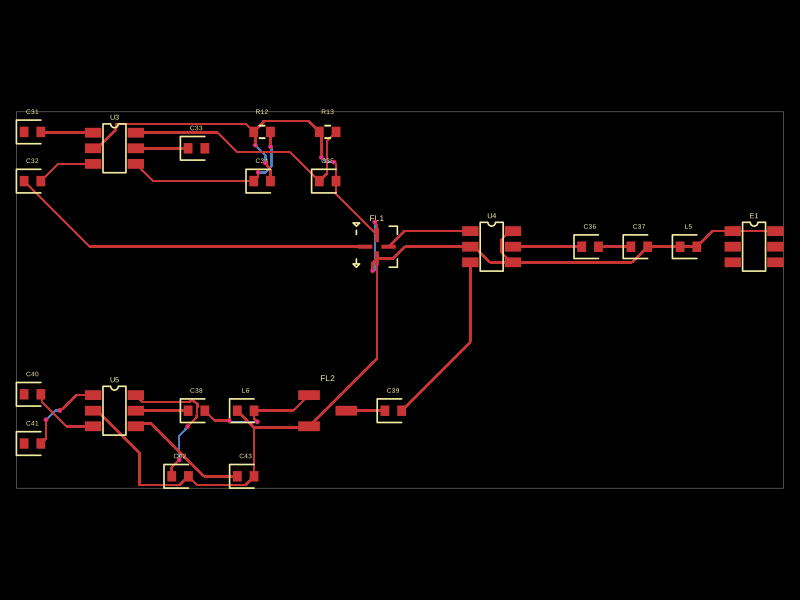 Similar packageMustafaMulla29/CC3235SF-tsxThis code defines a PCB layout with RF front-end components including RF switches (RTC6608OSP), band-pass filters, a diplexer, matching capacitors and inductors, and an antenna, all arranged to match a specific schematic for high-frequency radio signal routing.
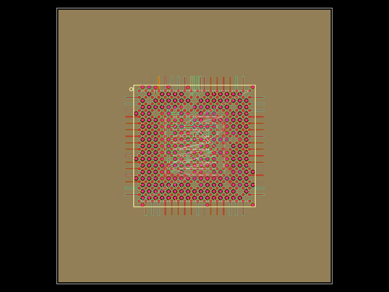 Discover something new0hmX/am3352This code defines a six-layer printed circuit board (PCB) design with a TI AM3352 microprocessor package, including precise pin mapping, power plane definition, fixed component placement, and PCB layout visualization.