imrishabh18/test-pcm
This code defines a 10mm by 10mm electronic circuit board containing a single pin-row chip with an associated 3D CAD model of the "MachineContactMedium" component.
- Version
- 1.0.3
- License
- unset
- Stars
- 0
dist/kicad-library/footprints/test-pcm.pretty/MyBoard.kicad_mod
(footprint
  "MyBoard"
  (layer F.Cu)
  (at 0 0 0)
  (descr "")
  (tags "")
  (attr through_hole)
  (embedded_fonts no)
  (property "Reference" "REF**"
    (at 0 -1.25 0)
    (layer F.SilkS)
    (uuid 521fe180-3a89-2d01-38cd-c47e53db4a03)
    (effects
      (font
        (size 1.27 1.27)
        (thickness 0.15)
      )
    )
  )
  (property "Value" "Val**"
    (at 0 1.25 0)
    (layer F.Fab)
    (uuid 59786640-408c-b2ff-256e-33c27496e57d)
    (effects
      (font
        (size 1.27 1.27)
        (thickness 0.15)
      )
    )
  )
  (property "Datasheet" ""
    (at 0 0 0)
    (layer F.Fab)
    (hide yes)
    (uuid 6b33c240-2175-4c41-51e1-a53e3ac76943)
    (effects
      (font
        (size 1.27 1.27)
        (thickness 0.15)
      )
    )
  )
  (property "Description" ""
    (at 0 0 0)
    (layer F.Fab)
    (hide yes)
    (uuid 06594860-0cf8-b6c1-1398-25221a379383)
    (effects
      (font
        (size 1.27 1.27)
        (thickness 0.15)
      )
    )
  )
  (fp_text
    user
    "pin1"
    (at 0 -1.125 0)
    (layer F.SilkS)
    (effects
      (font
        (size 0.3333333333333333 0.3333333333333333)
      )
    )
  )
  (fp_text
    reference
    "REF**"
    (at 0 -2.54 0)
    (layer F.SilkS)
    (effects
      (font
        (size 0.4666666666666666 0.4666666666666666)
      )
    )
  )
  (pad "1" thru_hole rect
    (at 0 0 0)
    (size 1.5 1.5)
    (drill 1)
    (layers *.Cu *.Mask)
    (uuid 633a4dec-1f37-b14c-24ca-eb5468cd87f4)
  )
  (model "../../3dmodels/test-pcm.3dshapes/MachineContactMedium.step"
    (offset
      (xyz 0 0 0.7)
    )
    (rotate
      (xyz 0 0 0)
    )
  )
)
Related Packages
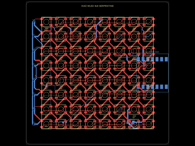 More from this authorimrishabh18/desk-led-matrixThis code models a hardware setup comprising a WLED-compatible LED cascade array connected to a XIAO ESP32-C3 microcontroller, including power regulation components and detailed PCB layout with traces, pads, and silkscreen markings.
 Similar packageMustafaMulla29/wireless-mouse-pcbThis code defines a 3.3V low dropout voltage regulator chip (AP2112K-3.3TRG1) with five pins (VIN, GND, Enable, NC, VOUT) and its associated PCB footprint and 3D models for hardware implementation.
 Discover something newhrithik18k/smart-switch-pcbThe AO3400A component models a SOT-23 N-channel MOSFET with labeled pins for Gate, Source, and Drain, including 3D CAD models and schematic symbols for electronic circuit design.