liammcg/BayFinder_V1_REVC_ESP32_CARRIER
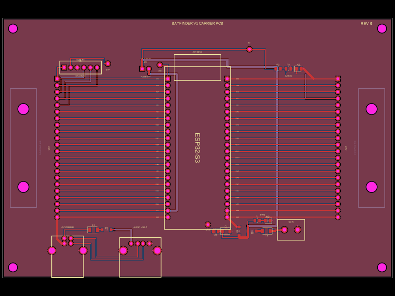
This design implements a control PCB assembly featuring multiple headers (J1–J4) for ESP32-S3 module connection, integrated USB Type-B and A connectors (J5, J6) for power and data, a protected 5V power circuitry with fuses and TVS diode, an onboard SSD1306 OLED display (J8), and mechanical DIN-rail mounting holes, all interconnected with signal traces, ground pours, and test points.
- Version
- 0.0.1
- License
- unset
- Stars
- 0
index.tsx
PCB
Schematic
import * as React from "react"
/*
* BAYFINDER BF-CTRL-PCB REV B — SELECTED PRODUCTION PARTS
*
* ESP socket rows:
* J1/J4 Sullins PRPC022SAAN-RC (5.84 mm mating length)
* J2/J3 Sullins PPPC221LFBN-RC (DigiKey S7055-ND)
*
* Display assembly:
* DS1 Adafruit 4440 SSD1306 128x32 OLED (DigiKey 1528-4440-ND)
* J8 Sullins PPPC061LGBN-RC 6-pin right-angle socket (DigiKey S5481-ND)
*
* Power and service connectors:
* J5 Amphenol 61729-0010BLF USB-B (DigiKey 609-1039-ND)
* J6 Molex 0676433910 USB-A receptacle (DigiKey WM14667-ND)
* J7 On Shore EDSTLZ950/2 5.08 mm header (DigiKey ED1817-ND)
* Mating field plug: EDZ950/2
* JP1 Sullins PRPC002SAAN-RC (DigiKey 35-PRPC002SAAN-RC-ND)
*
* DIN-rail mounting:
* CL1/2 Hammond 1427DINCLIP, black nylon 35 mm DIN-rail clips
* One package contains the two clips used on the PCB back side;
* each clip uses the documented 30 mm mounting-hole spacing.
*
* Off-board service cables:
* PC->J5 Eaton U023-006 USB-A male to USB-B male (DigiKey TL773-ND)
* J6->ESP Assmann AK67421-0.3-VM USB-A male to Micro-B male
* 300 mm cable (DigiKey AE11229-ND)
*
* Protection and indication:
* F1 Littelfuse 0468001.NR, 1 A / 63 V, 1206 (F2658CT-ND)
* F2 Littelfuse 0468.500NR, 0.5 A / 63 V, 1206 (F3156CT-ND)
* D1/D3 Diodes Inc. B140HW-7, 1 A / 40 V Schottky (B140HWDICT-ND)
* D2 Littelfuse SMF5.0A, 5 V TVS, SOD-123 (F5748CT-ND)
* C1 Murata GRM31CR61A476ME15L, 47 uF / 10 V, 1206 (490-5528-1-ND)
* C2/C3 Wurth 885012207098, 100 nF / 50 V, 0805 (732-8080-1-ND)
* R1 Vishay CRCW08051K00FKEA, 1 k, 0805 (541-1.00KCCT-ND)
* R2 Vishay CRCW0805100KFKEA, 100 k, 0805 (541-100KCCT-ND)
* R3 Vishay CRCW080568K0FKEA, 68 k, 0805 (541-68.0KCCT-ND)
* LED1 Wurth 150080GS75000, green 0805 (732-4983-1-ND)
*
* The 100 k / 68 k divider scales 5.25 V to about 2.13 V at GPIO1.
* Firmware conversion: input5V = adcVolts * (100.0 + 68.0) / 68.0.
*
* POWER-SOURCE RULE:
* Normal enclosure operation: install the JP1 shunt.
* PC USB maintenance: remove the JP1 shunt before connecting J5.
* Never power the ESP32-S3 from enclosure 5 V and USB simultaneously.
*/
const leftPins = [
"L_3V3_1",
"L_3V3_2",
"L_RST",
"L_GPIO4",
"L_GPIO5",
"L_GPIO6",
"L_GPIO7",
"L_GPIO15",
"L_GPIO16",
"L_GPIO17",
"L_GPIO18",
"L_GPIO8",
"L_GPIO3",
"L_GPIO46",
"L_GPIO9",
"L_GPIO10",
"L_GPIO11",
"L_GPIO12",
"L_GPIO13",
"L_GPIO14",
"L_5V",
"L_GND",
]
const rightPins = [
"R_GND_1",
"R_GPIO43_TX",
"R_GPIO44_RX",
"R_GPIO1",
"R_GPIO2",
"R_GPIO42",
"R_GPIO41",
"R_GPIO40",
"R_GPIO39",
"R_GPIO38",
"R_GPIO37_RESERVED",
"R_GPIO36_RESERVED",
"R_GPIO35_RESERVED",
"R_GPIO0_BOOT",
"R_GPIO45",
"R_GPIO48",
"R_GPIO47",
"R_GPIO21",
"R_GPIO20_USB_DP",
"R_GPIO19_USB_DM",
"R_GND_2",
"R_GND_3",
]
// Avoid String.padStart() so editors using an older JavaScript library target
// do not report a false compatibility error.
const twoDigit = (value) => (value < 10 ? `0${value}` : `${value}`)
const leftTraceNames = leftPins.map(
(_, index) => `LEFT_IO_${twoDigit(index + 1)}`,
)
const rightTraceNames = rightPins.map(
(_, index) => `RIGHT_IO_${twoDigit(index + 1)}`,
)
/*
* Each relocation trace is a short, direct horizontal connection.
* pcbStraightLine prevents the autorouter from producing unnecessary
* jogs or vias between the outer male headers and the ESP32 sockets.
*/
const leftTraces = leftPins.map((pin, index) => (
<trace
key={`L-${pin}`}
name={leftTraceNames[index]}
from={`J1.${pin}`}
to={`J2.${pin}`}
width="0.40mm"
pcbStraightLine
maxViaCount={pin.includes("GND") ? 1 : 0}
/>
))
const rightTraces = rightPins.map((pin, index) => (
<trace
key={`R-${pin}`}
name={rightTraceNames[index]}
from={`J3.${pin}`}
to={`J4.${pin}`}
width="0.40mm"
pcbStraightLine
maxViaCount={pin.includes("GND") ? 1 : 0}
/>
))
/*
* Short, human-readable ESP32-S3 pin names for the two female
* DevKit socket rows. Pin 1 is at the top of each vertical row.
*/
const j2SilkLabels = [
"3V3",
"3V3",
"RST",
"IO4",
"IO5",
"IO6",
"IO7",
"IO15",
"IO16",
"IO17",
"IO18",
"IO8",
"IO3",
"IO46",
"IO9",
"IO10",
"IO11",
"IO12",
"IO13",
"IO14",
"5V",
"GND",
]
const j3SilkLabels = [
"GND",
"TX0",
"RX0",
"IO1",
"IO2",
"IO42",
"IO41",
"IO40",
"IO39",
"IO38",
"IO37*",
"IO36*",
"IO35*",
"BOOT",
"IO45",
"IO48",
"IO47",
"IO21",
"USB+",
"USB-",
"GND",
"GND",
]
const espHeaderPinY = (index) => 26.67 - index * 2.54
const j2PinSilk = j2SilkLabels.map((label, index) => (
<silkscreentext
key={`J2-SILK-${index}`}
text={label}
pcbX={-15.4}
pcbY={espHeaderPinY(index)}
pcbRotation={0}
fontSize="0.55mm"
/>
))
const j3PinSilk = j3SilkLabels.map((label, index) => (
<silkscreentext
key={`J3-SILK-${index}`}
text={label}
pcbX={15.4}
pcbY={espHeaderPinY(index)}
pcbRotation={0}
fontSize="0.55mm"
/>
))
const makeThTestpointFootprint = () => (
<footprint>
<platedhole
portHints={["pin1"]}
pcbX="0mm"
pcbY="0mm"
shape="circle"
holeDiameter="1.02mm"
outerDiameter="2mm"
/>
<courtyardcircle
pcbX="0mm"
pcbY="0mm"
radius="1.25mm"
/>
</footprint>
)
/*
* Accurate 3D model for the stock-length, upward-facing J1/J4 headers.
*
* PRPC022SAAN-RC dimensions:
* 5.84 mm mating section above the 2.50 mm insulator
* 3.05 mm solder post below the insulator
* 11.39 mm overall contact length
*
* The black plastic carrier stays above the PCB, matching the orientation
* of the female socket rows. The footprint and pin locations are unchanged.
*/
const makeUpwardStockMaleHeaderCadModel = () => {
const pinCount = 22
const pitch = 2.54
const pinSize = 0.64
const bodyWidth = 2.54
const bodyHeight = 2.5
const matingLength = 5.84
const postLength = 3.05
const bodyLength = pinCount * pitch
const totalPinLength = postLength + bodyHeight + matingLength
const pinCenterZ =
(-postLength + bodyHeight + matingLength) / 2
const firstPinX = -((pinCount - 1) * pitch) / 2
const pins = Array.from({ length: pinCount }, (_, index) => ({
type: "colorize",
color: [0.88, 0.66, 0.12],
shape: {
type: "translate",
vector: [
firstPinX + index * pitch,
0,
pinCenterZ,
],
shape: {
type: "cuboid",
size: [
pinSize,
pinSize,
totalPinLength,
],
},
},
}))
return {
jscad: {
type: "union",
shapes: [
{
type: "colorize",
color: [0.05, 0.05, 0.05],
shape: {
type: "translate",
vector: [0, 0, bodyHeight / 2],
shape: {
type: "cuboid",
size: [
bodyLength,
bodyWidth,
bodyHeight,
],
},
},
},
...pins,
],
},
modelOriginPosition: {
x: 0,
y: 0,
z: 0,
},
modelBounds: {
min: {
x: -bodyLength / 2,
y: -bodyWidth / 2,
z: -postLength,
},
max: {
x: bodyLength / 2,
y: bodyWidth / 2,
z: bodyHeight + matingLength,
},
},
size: {
x: bodyLength,
y: bodyWidth,
z: totalPinLength,
},
modelBoardNormalDirection: "z+" as const,
}
}
const BayFinderCarrier = () => (
<board
name="BF_CTRL_REVB"
title="BayFinder Control PCB Rev B"
width="150mm"
height="100mm"
thickness="1.6mm"
layers={2}
material="fr4"
solderMaskColor="black"
silkscreenColor="white"
autorouter={{ preset: "auto" }}
defaultTraceWidth="0.25mm"
minTraceWidth="0.20mm"
minTraceToPadEdgeClearance="0.20mm"
minPadEdgeToPadEdgeClearance="0.20mm"
minViaEdgeToPadEdgeClearance="0.20mm"
minViaHoleEdgeToViaHoleEdgeClearance="0.20mm"
minPlatedHoleDrillEdgeToDrillEdgeClearance="0.25mm"
minBoardEdgeClearance="0.35mm"
schAutoLayoutEnabled
schTraceAutoLabelEnabled
pcbStyle={{ silkscreenFontSize: 0.8 }}
>
<schematicsheet
name="MAIN"
displayName="BayFinder Carrier Rev B"
/>
{/* J1 male | J2 female | ESP32-S3 | J3 female | J4 male */}
<pinheader
name="J1"
manufacturerPartNumber="PRPC022SAAN-RC"
pinCount={22}
pinLabels={leftPins}
gender="male"
connectsFromAbove
footprint="pinrow22_p2.54mm_id1.10mm_od1.80mm_male_invert_nopinlabels"
cadModel={makeUpwardStockMaleHeaderCadModel()}
pitch="2.54mm"
holeDiameter="1.1mm"
platedDiameter="1.8mm"
showSilkscreenPinLabels={false}
pcbStyle={{ silkscreenTextVisibility: "hidden" }}
pcbX={-54}
pcbY={0}
pcbRotation={-90}
/>
<pinheader
name="J2"
manufacturerPartNumber="PPPC221LFBN-RC"
pinCount={22}
pinLabels={leftPins}
gender="female"
pitch="2.54mm"
holeDiameter="1.1mm"
platedDiameter="1.8mm"
showSilkscreenPinLabels={false}
pcbStyle={{ silkscreenTextVisibility: "hidden" }}
pcbX={-11.43}
pcbY={0}
pcbRotation={-90}
/>
<pinheader
name="J3"
manufacturerPartNumber="PPPC221LFBN-RC"
pinCount={22}
pinLabels={rightPins}
gender="female"
pitch="2.54mm"
holeDiameter="1.1mm"
platedDiameter="1.8mm"
showSilkscreenPinLabels={false}
pcbStyle={{ silkscreenTextVisibility: "hidden" }}
pcbX={11.43}
pcbY={0}
pcbRotation={-90}
/>
<pinheader
name="J4"
manufacturerPartNumber="PRPC022SAAN-RC"
pinCount={22}
pinLabels={rightPins}
gender="male"
connectsFromAbove
footprint="pinrow22_p2.54mm_id1.10mm_od1.80mm_male_invert_nopinlabels"
cadModel={makeUpwardStockMaleHeaderCadModel()}
pitch="2.54mm"
holeDiameter="1.1mm"
platedDiameter="1.8mm"
showSilkscreenPinLabels={false}
pcbStyle={{ silkscreenTextVisibility: "hidden" }}
pcbX={54}
pcbY={0}
pcbRotation={-90}
/>
{j2PinSilk}
{j3PinSilk}
{leftTraces}
{rightTraces}
{/* Protected 5 V input */}
<connector
name="J7"
manufacturerPartNumber="EDSTLZ950/2"
pinLabels={{
pin1: "VIN",
pin2: "GND",
}}
pcbX={36}
pcbY={-31.5}
pcbRotation={0}
allowOffBoard
footprint={
<footprint insertionDirection="from_bottom">
<platedhole
portHints={["pin1", "VIN"]}
pcbX="-2.54mm"
pcbY="0mm"
shape="circle"
holeDiameter="1.4mm"
outerDiameter="2.4mm"
/>
<platedhole
portHints={["pin2", "GND"]}
pcbX="2.54mm"
pcbY="0mm"
shape="circle"
holeDiameter="1.4mm"
outerDiameter="2.4mm"
/>
<silkscreenrect
pcbX="0mm"
pcbY="0mm"
width="10.5mm"
height="8mm"
strokeWidth="0.25mm"
/>
<courtyardrect
pcbX="0mm"
pcbY="0mm"
width="11.5mm"
height="9mm"
/>
</footprint>
}
/>
<fuse
name="F1"
manufacturerPartNumber="0468001.NR"
currentRating="1A"
voltageRating="63V"
footprint="1206"
pcbX={26.5}
pcbY={-32}
pcbRotation={180}
/>
<diode
name="D1"
manufacturerPartNumber="B140HW-7"
variant="schottky"
footprint="sod123"
pcbX={21}
pcbY={-32}
pcbRotation={180}
/>
<diode
name="D2"
manufacturerPartNumber="SMF5.0A"
variant="tvs"
footprint="sod123"
pcbX={16}
pcbY={-32}
pcbRotation={90}
/>
<capacitor
name="C1"
manufacturerPartNumber="GRM31CR61A476ME15L"
capacitance="47uF"
footprint="1206"
pcbX={11}
pcbY={-32}
/>
<capacitor
name="C2"
manufacturerPartNumber="885012207098"
capacitance="0.1uF"
footprint="0805"
pcbX={7}
pcbY={-32}
pcbRotation={180}
/>
<trace
name="VIN_TO_F1"
from="J7.VIN"
to="F1.pin1"
width="0.80mm"
pcbStraightLine
maxViaCount={0}
/>
<trace
name="F1_TO_D1"
from="F1.pin2"
to="D1.pin1"
width="0.80mm"
pcbStraightLine
maxViaCount={0}
/>
<trace
name="J7_GND"
from="J7.GND"
to="net.GND"
width="0.80mm"
maxViaCount={1}
/>
{/* Protected 5 V distribution along the lower assembly edge. */}
<trace
name="PROT_5V_TVS"
from="D1.pin2"
to="D2.pin1"
width="0.80mm"
pcbPath={[
{ x: 1.65, y: 2.5 },
{ x: 5, y: 2.5 },
]}
maxViaCount={0}
/>
<trace
name="TVS_GND"
from="D2.pin2"
to="net.GND"
width="0.60mm"
/>
<trace
name="PROT_5V_BULK"
from="D2.pin1"
to="C1.pin1"
width="0.60mm"
pcbPath={[
{ x: -2.5, y: 0 },
{ x: -2.5, y: 6.46 },
]}
maxViaCount={0}
/>
<trace
name="C1_GND"
from="C1.pin2"
to="net.GND"
width="0.60mm"
/>
<trace
name="PROT_5V_DECOUPLE"
from="C1.pin1"
to="C2.pin1"
width="0.60mm"
pcbStraightLine
maxViaCount={0}
/>
<trace
name="C2_GND"
from="C2.pin2"
to="net.GND"
width="0.50mm"
/>
{/**
* Removable ESP32 5 V link. Install JP1 only for enclosure-powered use.
* Remove JP1 before attaching a computer to J5 so the DevKit never sees
* USB power and header 5 V at the same time.
*/}
<pinheader
name="JP1"
manufacturerPartNumber="PRPC002SAAN-RC"
pinCount={2}
pinLabels={{
pin1: "SYS",
pin2: "ESP",
}}
gender="male"
pitch="2.54mm"
holeDiameter="1.1mm"
platedDiameter="1.8mm"
showSilkscreenPinLabels={false}
pcbX={-20}
pcbY={30.5}
/>
<trace
name="PWR_5V_SYS"
from="JP1.SYS"
to="D1.pin2"
width="0.80mm"
pcbPathRelativeTo="JP1.SYS"
pcbPath={[
{ x: -1.27, y: 0 },
{ x: -1.27, y: 3.5 },
{
x: -1.27,
y: 3.5,
via: true,
fromLayer: "top",
toLayer: "bottom",
},
{ x: -1.27, y: 3.5 },
{ x: 31.5, y: 3.5 },
{ x: 31.5, y: 0.7 },
{ x: 50.5, y: 0.7 },
{ x: 50.5, y: -60.5 },
{ x: 39.35, y: -60.5 },
{
x: 39.35,
y: -60.5,
via: true,
fromLayer: "bottom",
toLayer: "top",
},
{ x: 39.35, y: -60.5 },
{ x: 39.35, y: -62.5 },
]}
maxViaCount={2}
/>
<trace
name="PWR_5V_ESP"
from="JP1.ESP"
to="J2.L_5V"
width="0.80mm"
pcbPathRelativeTo="JP1.ESP"
pcbPath={[
{ x: 1.27, y: 0 },
{ x: 1.27, y: -2 },
{
x: 1.27,
y: -2,
via: true,
fromLayer: "top",
toLayer: "bottom",
},
{ x: 1.27, y: -2 },
{ x: 12, y: -2 },
{ x: 12, y: -54.63 },
{ x: 8.57, y: -54.63 },
]}
maxViaCount={1}
/>
<trace
name="ESP_GND_L"
from="J2.L_GND"
to="net.GND"
width="0.80mm"
/>
<trace
name="ESP_GND_R1"
from="J3.R_GND_1"
to="net.GND"
width="0.80mm"
/>
<trace
name="ESP_GND_R2"
from="J3.R_GND_2"
to="net.GND"
width="0.80mm"
/>
<trace
name="ESP_GND_R3"
from="J3.R_GND_3"
to="net.GND"
width="0.80mm"
/>
{/**
* Amphenol 61729-0010BLF right-angle USB Type-B service connector.
* Released footprint: 2.50 x 2.00 mm signal grid, 12.04 mm shell-hole
* spacing, 1.00 mm signal drills, and 2.30 mm shell drills.
* The mating face is aligned with the lower PCB edge.
*/}
<connector
name="J5"
manufacturerPartNumber="61729-0010BLF"
pinLabels={{
pin1: "VBUS",
pin2: "DM",
pin3: "DP",
pin4: "UGND",
pin5: "SH1",
pin6: "SH2",
}}
pcbX={-50}
pcbY={-39.5}
pcbRotation={0}
allowOffBoard
footprint={
<footprint insertionDirection="from_bottom">
<platedhole
portHints={["pin1", "VBUS"]}
pcbX="-1.25mm"
pcbY="4.71mm"
shape="circle"
holeDiameter="1mm"
outerDiameter="1.8mm"
/>
<platedhole
portHints={["pin2", "DM"]}
pcbX="1.25mm"
pcbY="4.71mm"
shape="circle"
holeDiameter="1mm"
outerDiameter="1.8mm"
/>
<platedhole
portHints={["pin3", "DP"]}
pcbX="1.25mm"
pcbY="2.71mm"
shape="circle"
holeDiameter="1mm"
outerDiameter="1.8mm"
/>
<platedhole
portHints={["pin4", "UGND"]}
pcbX="-1.25mm"
pcbY="2.71mm"
shape="circle"
holeDiameter="1mm"
outerDiameter="1.8mm"
/>
<platedhole
portHints={["pin5", "SH1"]}
pcbX="-6.02mm"
pcbY="0mm"
shape="circle"
holeDiameter="2.3mm"
outerDiameter="3mm"
/>
<platedhole
portHints={["pin6", "SH2"]}
pcbX="6.02mm"
pcbY="0mm"
shape="circle"
holeDiameter="2.3mm"
outerDiameter="3mm"
/>
<silkscreenrect
pcbX="0mm"
pcbY="-2.4mm"
width="12.2mm"
height="16mm"
strokeWidth="0.25mm"
/>
<courtyardrect
pcbX="0mm"
pcbY="-2.4mm"
width="13.2mm"
height="17mm"
/>
</footprint>
}
/>
<fuse
name="F2"
manufacturerPartNumber="0468.500NR"
currentRating="0.5A"
voltageRating="63V"
footprint="1206"
pcbX={-40}
pcbY={-31.5}
/>
<diode
name="D3"
manufacturerPartNumber="B140HW-7"
variant="schottky"
footprint="sod123"
pcbX={-35}
pcbY={-31.5}
/>
{/**
* Molex 0676433910 right-angle USB Type-A service receptacle.
* Released footprint: signal x = -3.50, -1.00, +1.00, +3.50 mm;
* signal y = +2.71 mm; 0.95 mm signal drills; shell x = +/-6.57 mm;
* 2.30 mm shell drills. The mating face is aligned with the lower edge.
*/}
<connector
name="J6"
manufacturerPartNumber="0676433910"
pinLabels={{
pin1: "U5V",
pin2: "DM",
pin3: "DP",
pin4: "UGND",
pin5: "SH1",
pin6: "SH2",
}}
pcbX={-22}
pcbY={-39.5}
pcbRotation={180}
allowOffBoard
footprint={
<footprint insertionDirection="from_top">
<platedhole
portHints={["pin1", "U5V"]}
pcbX="3.5mm"
pcbY="-2.71mm"
shape="circle"
holeDiameter="0.95mm"
outerDiameter="1.8mm"
/>
<platedhole
portHints={["pin2", "DM"]}
pcbX="1mm"
pcbY="-2.71mm"
shape="circle"
holeDiameter="0.95mm"
outerDiameter="1.8mm"
/>
<platedhole
portHints={["pin3", "DP"]}
pcbX="-1mm"
pcbY="-2.71mm"
shape="circle"
holeDiameter="0.95mm"
outerDiameter="1.8mm"
/>
<platedhole
portHints={["pin4", "UGND"]}
pcbX="-3.5mm"
pcbY="-2.71mm"
shape="circle"
holeDiameter="0.95mm"
outerDiameter="1.8mm"
/>
<platedhole
portHints={["pin5", "SH1"]}
pcbX="6.57mm"
pcbY="0mm"
shape="circle"
holeDiameter="2.3mm"
outerDiameter="3.2mm"
/>
<platedhole
portHints={["pin6", "SH2"]}
pcbX="-6.57mm"
pcbY="0mm"
shape="circle"
holeDiameter="2.3mm"
outerDiameter="3.2mm"
/>
<silkscreenrect
pcbX="0mm"
pcbY="2.65mm"
width="16mm"
height="15.26mm"
strokeWidth="0.25mm"
/>
<courtyardrect
pcbX="0mm"
pcbY="2.65mm"
width="16.5mm"
height="16.26mm"
/>
</footprint>
}
/>
<trace
name="USB_VBUS_IN"
from="J5.VBUS"
to="F2.pin1"
width="0.40mm"
pcbPathRelativeTo="J5.VBUS"
pcbPath={[
{ x: -1.25, y: 4.71 },
{ x: -1.25, y: 8 },
{ x: 8.5375, y: 8 },
]}
maxViaCount={0}
/>
<trace
name="USB_VBUS_FUSED"
from="F2.pin2"
to="D3.pin1"
width="0.60mm"
pcbStraightLine
maxViaCount={0}
/>
<trace
name="USB_VBUS_OUT"
from="D3.pin2"
to="J6.U5V"
width="0.60mm"
pcbPathRelativeTo="D3.pin2"
pcbPath={[
{ x: 1.65, y: 0 },
{ x: 3, y: 0 },
{
x: 3,
y: 0,
via: true,
fromLayer: "top",
toLayer: "bottom",
},
{ x: 3, y: 0 },
{ x: 9.5, y: 0 },
{ x: 9.5, y: -5.29 },
]}
maxViaCount={1}
/>
<trace
name="USB_DM"
from="J5.DM"
to="J6.DM"
width="0.25mm"
pcbPathRelativeTo="J5.DM"
pcbPath={[
{ x: 1.25, y: 4.71 },
{ x: 11, y: 4.71 },
{ x: 11, y: -2.5 },
{ x: 27, y: -2.5 },
{ x: 27, y: 2.71 },
]}
maxViaCount={0}
/>
<trace
name="USB_DP"
from="J5.DP"
to="J6.DP"
width="0.25mm"
pcbPathRelativeTo="J5.DP"
pcbPath={[
{ x: 1.25, y: 2.71 },
{ x: 9, y: 2.71 },
{ x: 9, y: -3.5 },
{ x: 29, y: -3.5 },
{ x: 29, y: 2.71 },
]}
maxViaCount={0}
/>
<trace
name="USB_GND_IN"
from="J5.UGND"
to="net.GND"
width="0.60mm"
/>
<trace
name="USB_IN_SHIELD_1"
from="J5.SH1"
to="net.GND"
width="0.60mm"
/>
<trace
name="USB_IN_SHIELD_2"
from="J5.SH2"
to="net.GND"
width="0.60mm"
/>
<trace
name="USB_GND_OUT"
from="J6.UGND"
to="net.GND"
width="0.60mm"
/>
<trace
name="USB_SHIELD_1"
from="J6.SH1"
to="net.GND"
width="0.60mm"
/>
<trace
name="USB_SHIELD_2"
from="J6.SH2"
to="net.GND"
width="0.60mm"
/>
{/*
* USB Full-Speed service pair: short top-layer routes, 0.25 mm width,
* separated fan-in, and zero vias. Recalculate true 90-ohm differential
* geometry from the selected fabricator's production stackup.
*/}
{/*
* DS1 is an Adafruit 4440 SSD1306 OLED breakout. J8 is the carrier's
* 1x6 right-angle female socket. Fit a straight 1x6 male header to DS1,
* then plug the OLED directly onto J8. The display stands vertically at
* the carrier's top edge, so it does not cover ESP32 or relocation pads.
*/}
<pinheader
name="J8"
manufacturerPartNumber="PPPC061LGBN-RC"
pinCount={6}
pinLabels={[
"VIN",
"3VO",
"GND",
"RST",
"SCL",
"SDA",
]}
gender="female"
rightAngle
pitch="2.54mm"
holeDiameter="1.1mm"
platedDiameter="1.8mm"
showSilkscreenPinLabels={false}
pcbX={-45}
pcbY={31}
pcbRotation={0}
/>
<trace
name="OLED_3V3"
from="J8.VIN"
to="J1.L_3V3_1"
width="0.40mm"
pcbPathRelativeTo="J8.VIN"
pcbPath={[
{ x: -6.35, y: 0 },
{ x: -9, y: 0 },
{ x: -9, y: -4.33 },
]}
maxViaCount={0}
/>
<trace
name="OLED_3VO_TEST"
from="J8.3VO"
to="TP5.pin1"
width="0.30mm"
pcbPathRelativeTo="J8.3VO"
pcbPath={[
{ x: -3.81, y: 0 },
{ x: -3.81, y: 3.5 },
{ x: 9, y: 3.5 },
{ x: 9, y: 1.5 },
]}
maxViaCount={0}
/>
<trace
name="OLED_GND"
from="J8.GND"
to="net.GND"
width="0.40mm"
/>
<trace
name="OLED_RST"
from="J8.RST"
to="J1.L_RST"
width="0.20mm"
pcbPathRelativeTo="J8.RST"
pcbPath={[
{ x: 1.27, y: -1.2 },
{
x: 1.27,
y: -1.2,
via: true,
fromLayer: "top",
toLayer: "bottom",
},
{ x: 1.27, y: -1.2 },
{ x: 1.27, y: -4 },
{ x: -7.5, y: -4 },
{ x: -7.5, y: -9.41 },
]}
maxViaCount={1}
/>
<trace
name="OLED_SCL"
from="J8.SCL"
to="J1.L_GPIO4"
width="0.20mm"
pcbPathRelativeTo="J8.SCL"
pcbPath={[
{ x: 3.81, y: -1.2 },
{
x: 3.81,
y: -1.2,
via: true,
fromLayer: "top",
toLayer: "bottom",
},
{ x: 3.81, y: -1.2 },
{ x: 3.81, y: -5.5 },
{ x: -6, y: -5.5 },
{ x: -6, y: -11.95 },
]}
maxViaCount={1}
/>
<trace
name="OLED_SDA"
from="J8.SDA"
to="J1.L_GPIO5"
width="0.20mm"
pcbPathRelativeTo="J8.SDA"
pcbPath={[
{ x: 6.35, y: -1.2 },
{
x: 6.35,
y: -1.2,
via: true,
fromLayer: "top",
toLayer: "bottom",
},
{ x: 6.35, y: -1.2 },
{ x: 6.35, y: -7 },
{ x: -4.5, y: -7 },
{ x: -4.5, y: -14.49 },
]}
maxViaCount={1}
/>
{/* Right-angle connector body / vertical-display assembly marker. */}
<silkscreenrect
pcbX={-45}
pcbY={31}
width="16mm"
height="5mm"
strokeWidth="0.25mm"
/>
<silkscreentext
text="DS1 OLED"
pcbX={-45}
pcbY={27.8}
pcbRotation={0}
fontSize="0.8mm"
/>
{/*
* Protected-5-V monitor. GPIO1/ADC1_CH0 reads the divider and firmware
* writes the resulting voltage to DS1. At 5.25 V, VSNS is 2.125 V.
* Never change R3 to a value that can put more than 3.3 V on GPIO1.
*/}
<resistor
name="R2"
manufacturerPartNumber="CRCW0805100KFKEA"
resistance="100k"
footprint="0805"
pcbX={31}
pcbY={30.5}
/>
<resistor
name="R3"
manufacturerPartNumber="CRCW080568K0FKEA"
resistance="68k"
footprint="0805"
pcbX={35}
pcbY={30.5}
/>
<capacitor
name="C3"
manufacturerPartNumber="885012207098"
capacitance="0.1uF"
footprint="0805"
pcbX={39}
pcbY={30.5}
/>
<trace
name="VSNS_FEED"
from="TP1.pin1"
to="R2.pin1"
width="0.30mm"
pcbPathRelativeTo="TP1.pin1"
pcbPath={[
{ x: 0, y: 0 },
{ x: 6, y: 0 },
{ x: 6, y: -7.5 },
{ x: 10.0875, y: -7.5 },
]}
maxViaCount={0}
/>
<trace
name="VSNS_DIV"
from="R2.pin2"
to="R3.pin1"
width="0.25mm"
pcbStraightLine
maxViaCount={0}
/>
<trace
name="VSNS_FILTER"
from="R3.pin1"
to="C3.pin1"
width="0.25mm"
pcbPathRelativeTo="R3.pin1"
pcbPath={[
{ x: -0.9125, y: 0 },
{ x: -0.9125, y: -2 },
{ x: 3.0875, y: -2 },
{ x: 3.0875, y: 0 },
]}
maxViaCount={0}
/>
<trace
name="VSNS_ADC"
from="C3.pin1"
to="J4.R_GPIO1"
width="0.25mm"
pcbPathRelativeTo="C3.pin1"
pcbPath={[
{ x: -0.9125, y: 0 },
{ x: -0.9125, y: -2 },
{ x: 2.5, y: -2 },
{
x: 2.5,
y: -2,
via: true,
fromLayer: "top",
toLayer: "bottom",
},
{ x: 2.5, y: -2 },
{ x: 2.5, y: -11.45 },
{ x: 15, y: -11.45 },
]}
maxViaCount={1}
/>
<trace
name="VSNS_R_GND"
from="R3.pin2"
to="net.GND"
width="0.35mm"
/>
<trace
name="VSNS_C_GND"
from="C3.pin2"
to="net.GND"
width="0.35mm"
/>
{/* Power LED */}
<resistor
name="R1"
manufacturerPartNumber="CRCW08051K00FKEA"
resistance="1k"
footprint="0805"
pcbX={23}
pcbY={-28}
/>
<led
name="IND"
manufacturerPartNumber="150080GS75000"
color="green"
footprint="led0805"
pcbX={27}
pcbY={-28}
/>
<trace
name="PWR_LED_FEED"
from="R1.pin1"
to="D1.pin2"
width="0.25mm"
pcbPathRelativeTo="R1.pin1"
pcbPath={[
{ x: -0.9125, y: 0 },
{ x: -3.65, y: 0 },
{ x: -3.65, y: -4 },
]}
maxViaCount={0}
/>
<trace
name="PWR_LED_SERIES"
from="R1.pin2"
to="IND.pin1"
width="0.35mm"
pcbStraightLine
maxViaCount={0}
/>
<trace
name="PWR_LED_GND"
from="IND.pin2"
to="net.GND"
width="0.35mm"
/>
{/* Test points */}
<testpoint
name="TP1"
manufacturerPartNumber="5000"
footprint={makeThTestpointFootprint()}
pcbX={20}
pcbY={38}
/>
<testpoint
name="TP2"
manufacturerPartNumber="5000"
footprint={makeThTestpointFootprint()}
pcbX={-14.5}
pcbY={32}
/>
<testpoint
name="TP4"
manufacturerPartNumber="5000"
footprint={makeThTestpointFootprint()}
pcbX={4}
pcbY={-29.5}
/>
<testpoint
name="TP5"
manufacturerPartNumber="5000"
footprint={makeThTestpointFootprint()}
pcbX={-34.5}
pcbY={32.5}
/>
<trace
name="TP_5V"
from="JP1.SYS"
to="TP1.pin1"
width="0.50mm"
pcbPathRelativeTo="JP1.SYS"
pcbPath={[
{ x: -1.27, y: 0 },
{ x: -1.27, y: 7.5 },
{ x: 40, y: 7.5 },
]}
maxViaCount={0}
/>
<trace
name="TP_3V3"
from="TP2.pin1"
to="J2.L_3V3_1"
width="0.40mm"
pcbPathRelativeTo="TP2.pin1"
pcbPath={[
{ x: 0, y: 0 },
{ x: 3.07, y: 0 },
{ x: 3.07, y: -5.33 },
]}
maxViaCount={0}
/>
<trace
name="TP_GND"
from="TP4.pin1"
to="net.GND"
width="0.50mm"
/>
{/*
* Corner mounting holes: M3 clearance.
* Each hole is inside a custom footprint so TSCircuit has an explicit
* mechanical courtyard. The holes remain non-plated and non-conductive.
*/}
<chip
name="H1"
noSchematicRepresentation
pcbX={-71}
pcbY={46}
footprint={
<footprint>
<hole
diameter="3.2mm"
pcbX={0}
pcbY={0}
/>
<courtyardcircle
pcbX={0}
pcbY={0}
radius={3.5}
strokeWidth={0.1}
/>
</footprint>
}
/>
<chip
name="H2"
noSchematicRepresentation
pcbX={71}
pcbY={46}
footprint={
<footprint>
<hole
diameter="3.2mm"
pcbX={0}
pcbY={0}
/>
<courtyardcircle
pcbX={0}
pcbY={0}
radius={3.5}
strokeWidth={0.1}
/>
</footprint>
}
/>
<chip
name="H3"
noSchematicRepresentation
pcbX={-71}
pcbY={-46}
footprint={
<footprint>
<hole
diameter="3.2mm"
pcbX={0}
pcbY={0}
/>
<courtyardcircle
pcbX={0}
pcbY={0}
radius={3.5}
strokeWidth={0.1}
/>
</footprint>
}
/>
<chip
name="H4"
noSchematicRepresentation
pcbX={71}
pcbY={-46}
footprint={
<footprint>
<hole
diameter="3.2mm"
pcbX={0}
pcbY={0}
/>
<courtyardcircle
pcbX={0}
pcbY={0}
radius={3.5}
strokeWidth={0.1}
/>
</footprint>
}
/>
{/*
* Back-side 35 mm DIN-rail clip mounting for the pair of Hammond
* 1427DINCLIP clips. Each clip is 10.1 x 45.7 mm with 30 mm hole
* spacing. Keeping both clips outside J1/J4 avoids every signal route
* and supports the carrier at both ends of a horizontal DIN rail.
* Use low-profile #6/M3.5 hardware and insulating washers.
*/}
<chip
name="DIN_L1"
noSchematicRepresentation
pcbX={-67}
pcbY={15}
footprint={
<footprint>
<hole
diameter="4mm"
pcbX={0}
pcbY={0}
/>
<courtyardcircle
pcbX={0}
pcbY={0}
radius={4.5}
strokeWidth={0.1}
/>
</footprint>
}
/>
<chip
name="DIN_L2"
noSchematicRepresentation
pcbX={-67}
pcbY={-15}
footprint={
<footprint>
<hole
diameter="4mm"
pcbX={0}
pcbY={0}
/>
<courtyardcircle
pcbX={0}
pcbY={0}
radius={4.5}
strokeWidth={0.1}
/>
</footprint>
}
/>
<chip
name="DIN_R1"
noSchematicRepresentation
pcbX={67}
pcbY={15}
footprint={
<footprint>
<hole
diameter="4mm"
pcbX={0}
pcbY={0}
/>
<courtyardcircle
pcbX={0}
pcbY={0}
radius={4.5}
strokeWidth={0.1}
/>
</footprint>
}
/>
<chip
name="DIN_R2"
noSchematicRepresentation
pcbX={67}
pcbY={-15}
footprint={
<footprint>
<hole
diameter="4mm"
pcbX={0}
pcbY={0}
/>
<courtyardcircle
pcbX={0}
pcbY={0}
radius={4.5}
strokeWidth={0.1}
/>
</footprint>
}
/>
<silkscreenrect
pcbX={-67}
pcbY={0}
width="10.1mm"
height="45.7mm"
strokeWidth="0.25mm"
layer="bottom"
/>
<silkscreenrect
pcbX={67}
pcbY={0}
width="10.1mm"
height="45.7mm"
strokeWidth="0.25mm"
layer="bottom"
/>
<silkscreentext
text="DIN CLIP 30 C-C"
pcbX={-60.5}
pcbY={0}
pcbRotation={90}
fontSize="0.7mm"
layer="bottom"
/>
<silkscreentext
text="DIN CLIP 30 C-C"
pcbX={60.5}
pcbY={0}
pcbRotation={90}
fontSize="0.7mm"
layer="bottom"
/>
{/**
* Solid FR-4 is retained beneath the ESP32-S3 antenna end. This outline
* is an assembly marker only; it does not remove board material and does
* not block traces. Keep tall metal hardware out of the marked region.
*/}
<silkscreenrect
pcbX={0}
pcbY={31}
width="18mm"
height="10mm"
strokeWidth="0.25mm"
/>
{/*
* Bottom is the primary uninterrupted return plane. The top pour
* fills unused copper while preserving routing and pad clearance.
*/}
<copperpour
name="GND_BOTTOM"
layer="bottom"
connectsTo="net.GND"
unbroken
clearance="0.25mm"
padMargin="0.25mm"
traceMargin="0.25mm"
boardEdgeMargin="0.50mm"
cutoutMargin="0.30mm"
useThermalReliefs
coveredWithSolderMask
/>
<copperpour
name="GND_TOP"
layer="top"
connectsTo="net.GND"
clearance="0.25mm"
padMargin="0.25mm"
traceMargin="0.25mm"
boardEdgeMargin="0.50mm"
cutoutMargin="0.30mm"
useThermalReliefs
coveredWithSolderMask
/>
{/* Minimal assembly silkscreen */}
<silkscreentext
text="BAYFINDER V1 CARRIER PCB"
pcbX={0}
pcbY={48}
fontSize="1.4mm"
/>
<silkscreentext
text="REV B"
pcbX={65}
pcbY={48}
fontSize="1.5mm"
/>
<silkscreenrect
pcbX={0}
pcbY={0}
width="25.4mm"
height="62.74mm"
strokeWidth="0.25mm"
/>
<silkscreentext
text="ESP32-S3"
pcbX={0}
pcbY={0}
pcbRotation={-90}
fontSize="2.5mm"
/>
<silkscreentext
text="OUT"
pcbX={-57.2}
pcbY={0}
pcbRotation={90}
/>
<silkscreentext
text="OUT"
pcbX={57.2}
pcbY={0}
pcbRotation={90}
/>
<silkscreentext
text="J5 PC USB-B"
pcbX={-50}
pcbY={-30.5}
/>
<silkscreentext
text="J6 ESP USB-A"
pcbX={-22}
pcbY={-30.5}
/>
<silkscreentext
text="5V IN"
pcbX={36}
pcbY={-28.5}
/>
<silkscreentext
text="PWR"
pcbX={25}
pcbY={-25.8}
/>
<silkscreentext
text="OLED RA"
pcbX={-45}
pcbY={34}
fontSize="0.7mm"
/>
<silkscreentext
text="JP1 RUN=ON"
pcbX={-20}
pcbY={34.5}
fontSize="0.65mm"
/>
<silkscreentext
text="PC USB=OFF"
pcbX={-20}
pcbY={27.5}
fontSize="0.65mm"
/>
<silkscreentext
text="5V MON"
pcbX={35}
pcbY={27.8}
fontSize="0.7mm"
/>
<silkscreentext
text="5V"
pcbX={20}
pcbY={40.5}
fontSize="0.7mm"
/>
<silkscreentext
text="3V3"
pcbX={-14.5}
pcbY={29.8}
fontSize="0.7mm"
/>
<silkscreentext
text="GND"
pcbX={4}
pcbY={-31.5}
fontSize="0.7mm"
/>
<silkscreentext
text="O3V"
pcbX={-34.5}
pcbY={30.2}
fontSize="0.7mm"
/>
<silkscreentext
text="5V"
pcbX={-25.5}
pcbY={-34.6}
fontSize="0.55mm"
/>
<silkscreentext
text="D-"
pcbX={-23}
pcbY={-34.6}
fontSize="0.55mm"
/>
<silkscreentext
text="D+"
pcbX={-21}
pcbY={-34.6}
fontSize="0.55mm"
/>
<silkscreentext
text="G"
pcbX={-18.5}
pcbY={-34.6}
fontSize="0.55mm"
/>
<silkscreentext
text="ANT ZONE"
pcbX={0}
pcbY={37}
fontSize="0.7mm"
/>
</board>
)
export default BayFinderCarrierRelated Packages
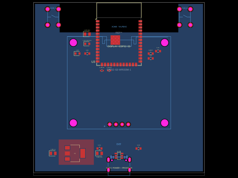 Similar packagegokul/board-v2This design integrates an ESP32-S3 Wi-Fi and Bluetooth module, a USB-C port with power and data circuitry, a USB ESD protection chip, a 3.3V voltage regulator, and an OLED display module on a PCB with associated routing and thermal copper pour layers.
 Discover something newhrithik18k/smart-switch-pcbThe AO3400A component models a SOT-23 N-channel MOSFET with labeled pins for Gate, Source, and Drain, including 3D CAD models and schematic symbols for electronic circuit design.