rushabhcodes/ESP32-E-Reader
This code defines the physical layout and schematic wiring of an ESP32-based e-reader device, including various surface-mount components such as connectors, ICs, resistors, capacitors, inductors, diodes, pushbuttons, and an antenna, with precise PCB placement and interconnection details.
- Version
- 1.0.8
- License
- unset
- Stars
- 0
index.circuit.tsx
PCB
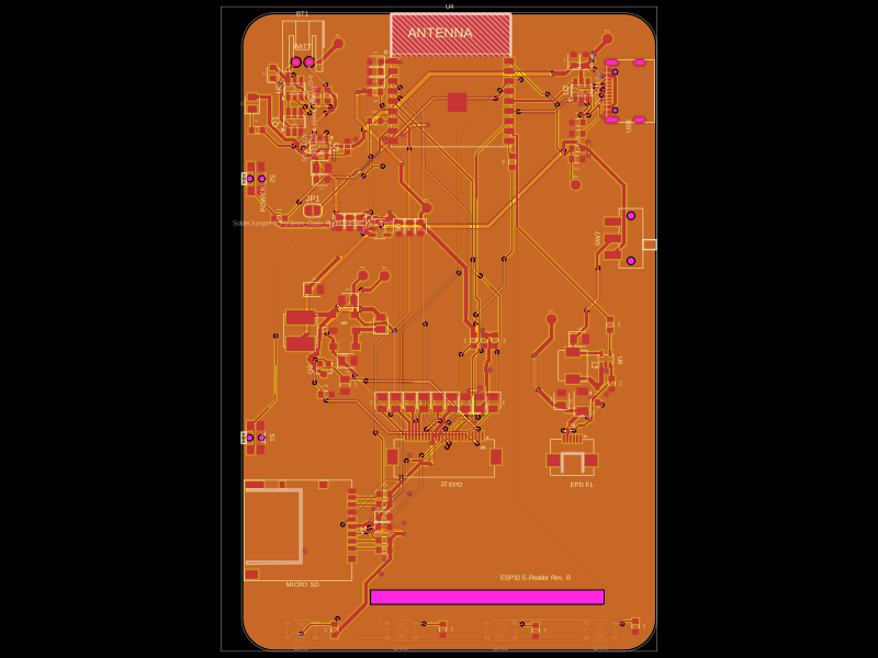
Schematic

/**
 * ESP32 E-Reader Rev. B
 *
 * Board-level composition. Electrical data and exact PCB placements live in
 * design-data.ts; functional blocks live in circuit-sections.tsx.
 */

import { Fragment } from "react";
import { CircuitSections } from "./circuit-sections";
import { nets, traceThicknessByNet } from "./design-data";

export default function ESP32EReader() {
	return (
		<board
			title="ESP32 E-Reader Rev. B"
			width="62.5mm"
			height="96.16mm"
			borderRadius="5mm"
			layers={4}
			thickness="1.6mm"
			doubleSidedAssembly
			minViaHoleDiameter="0.2mm"
			minViaPadDiameter="0.42mm"
			// 0.1 mm copper clearance + 0.11 mm annulus gives 0.21 mm
			// drill-to-trace clearance, above JLCPCB's 0.2 mm minimum.
			minTraceToPadEdgeClearance="0.1mm"
			autorouter={{ preset: "auto-local", allowViaInPad: false }}
		>
			{/* ESP32-C3-WROOM-02 antenna zone: no copper or routing on either side. */}
			<keepout
				shape="rect"
				width="18.2mm"
				height="6.65mm"
				pcbX={0.25}
				pcbY={44.755}
				layers={["top", "inner1", "inner2", "bottom"]}
			/>

			<CircuitSections />

			{Object.entries(nets).map(([name, connections]) => (
				<Fragment key={name}>
					<net
						name={name}
						isGroundNet={name === "GND"}
						isPowerNet={["GND", "V3V3", "USB_VBUS", "BATT_P"].includes(name)}
					/>
					{connections.map((connection, index) => (
						<Fragment key={`${name}-${index}`}>
							<trace
								from={connection}
								to={`net.${name}`}
								thickness={traceThicknessByNet[name] ?? "0.2mm"}
							/>
						</Fragment>
					))}
				</Fragment>
			))}

			{/* Four-layer fills provide short returns and a dedicated 3.3 V plane. */}
			<copperpour
				name="GND_FILL_TOP"
				connectsTo="net.GND"
				layer="top"
				clearance="0.2mm"
				boardEdgeMargin="0.3mm"
			/>
			<copperpour
				name="GND_FILL_BOTTOM"
				connectsTo="net.GND"
				layer="bottom"
				clearance="0.2mm"
				boardEdgeMargin="0.3mm"
			/>
			<copperpour
				name="GND_PLANE_INNER1"
				connectsTo="net.GND"
				layer="inner1"
				clearance="0.2mm"
				boardEdgeMargin="0.3mm"
			/>
			<copperpour
				name="V3V3_PLANE_INNER2"
				connectsTo="net.V3V3"
				layer="inner2"
				clearance="0.2mm"
				boardEdgeMargin="0.3mm"
			/>

			<cutout
				name="ENCLOSURE_SLOT"
				shape="rect"
				width="35mm"
				height="2mm"
				pcbX={5.75}
				pcbY={-39.92}
			/>

			<silkscreentext text="BATT" pcbX={-22} pcbY={43} fontSize="1mm" />
			<silkscreentext
				text="USB"
				pcbX={27}
				pcbY={31}
				pcbRotation={90}
				fontSize="1mm"
			/>
			<silkscreentext
				text="POWER"
				pcbX={-28}
				pcbY={20}
				pcbRotation={90}
				fontSize="1mm"
			/>
			<silkscreentext
				text="EN"
				pcbX={-28}
				pcbY={-16}
				pcbRotation={90}
				fontSize="1mm"
			/>
			<silkscreentext text="EPD" pcbX={1} pcbY={-23} fontSize="1mm" />
			<silkscreentext text="EPD FL" pcbX={20} pcbY={-23} fontSize="1mm" />
			<silkscreentext text="MICRO SD" pcbX={-22} pcbY={-38} fontSize="1mm" />
			<silkscreentext
				text="ESP32 E-Reader  Rev. B"
				pcbX={13}
				pcbY={-37}
				fontSize="1mm"
			/>
		</board>
	);
}
Related Packages
 More from this authorrushabhcodes/tetrisThis code defines various electronic component models—including a AAA battery holder, ATtiny85 microcontroller, switch, buzzer, display, and resistors—as hardware modules with detailed footprints, pin configurations, CAD models, and physical specifications for use in circuit design.
 Similar packageShiboSoftwareDev/i-wanThis code defines a PCB and schematic for a microcontroller development board, incorporating various surface-mount components (resistors, capacitors, headers, connectors, crystals, and an IC), with detailed footprints, electrical nets, and routing instructions.
 Discover something newimrishabh18/fitness_watchThis circuit integrates an ESP-12E microcontroller with various sensors, relays, and power management components, including an AO3400A transistor for switching loads, to enable wireless control and sensing functions.