tscircuit/autorouting-dataset-01
This code manages the hardware and electronic components for circuit design and PCB layout, defining components like resistors, capacitors, transistors, connectors, and footprints, and providing tools for component placement, PCB topology, and electrical connections.
- Version
- 1.0.102
- License
- unset
- Stars
- 4
lib/circuit/circuit020.tsx
PCB

Schematic

/** QRE1113 analog line sensor breakout with labeled silkscreen and 3-pin header. */
import { sel } from "@tscircuit/core"
import { shouldAutorouterRun } from "lib/shouldAutorouterRun"
export const JP1_FOOTPRINT = (
  <footprint>
    <smtpad
      portHints={["pin3"]}
      pcbX="-2.54mm"
      pcbY="5mm"
      width="1mm"
      height="3mm"
      shape="rect"
    />
    <smtpad
      portHints={["pin2"]}
      pcbX="0mm"
      pcbY="5mm"
      width="1mm"
      height="3mm"
      shape="rect"
    />
    <smtpad
      portHints={["pin1"]}
      pcbX="2.54mm"
      pcbY="5mm"
      width="1mm"
      height="3mm"
      shape="rect"
    />
  </footprint>
)

export const U1_FOOTPRINT = (
  <footprint>
    <smtpad
      portHints={["pin1"]}
      pcbX="-1.8mm"
      pcbY="-0.9mm"
      width="1.2mm"
      height="0.6mm"
      shape="rect"
    />
    <smtpad
      portHints={["pin2"]}
      pcbX="1.8mm"
      pcbY="-0.9mm"
      width="1.2mm"
      height="0.6mm"
      shape="rect"
    />
    <smtpad
      portHints={["pin3"]}
      pcbX="1.8mm"
      pcbY="0.9mm"
      width="1.2mm"
      height="0.6mm"
      shape="rect"
    />
    <smtpad
      portHints={["pin4"]}
      pcbX="-1.8mm"
      pcbY="0.9mm"
      width="1.2mm"
      height="0.6mm"
      shape="rect"
    />
  </footprint>
)

export const R_FOOTPRINT = (
  <footprint>
    <smtpad
      portHints={["pin1"]}
      pcbX="-0.65mm"
      pcbY="0mm"
      width="0.7mm"
      height="0.9mm"
      shape="rect"
    />
    <smtpad
      portHints={["pin2"]}
      pcbX="0.65mm"
      pcbY="0mm"
      width="0.7mm"
      height="0.9mm"
      shape="rect"
    />
  </footprint>
)
export default () => (
  <board
    routingDisabled={!shouldAutorouterRun()}
    width="7.62mm"
    height="24.13mm"
  >
    <pinheader
      gender="female"
      footprint={JP1_FOOTPRINT}
      pinCount={3}
      name="JP1"
      schPinArrangement={{
        rightSide: {
          direction: "bottom-to-top",
          pins: [1, 2, 3],
        },
      }}
      connections={{
        pin3: sel.R2.pin1,
      }}
      pcbY={-0.97}
      pcbRotation={180}
      layer="bottom"
    />
    <silkscreentext
      text="GND"
      fontSize={1}
      pcbY={-3}
      pcbX={2.4}
      pcbRotation={90}
    />
    <silkscreentext
      text="VCC"
      fontSize={1}
      pcbY={-3}
      pcbX={-0.1}
      pcbRotation={90}
    />
    <silkscreentext
      text="OUT"
      fontSize={1}
      pcbY={-3}
      pcbX={-2.6}
      pcbRotation={90}
    />
    <silkscreentext
      text="OUT"
      fontSize={1}
      pcbY={-3}
      pcbX={2.4}
      pcbRotation={90}
      layer="bottom"
    />
    <silkscreentext
      text="VCC"
      fontSize={1}
      pcbY={-3}
      pcbX={-0.1}
      pcbRotation={90}
      layer="bottom"
    />
    <silkscreentext
      text="GND"
      fontSize={1}
      pcbY={-3}
      pcbX={-2.6}
      pcbRotation={90}
      layer="bottom"
    />
    <netlabel
      net="GND"
      anchorSide="top"
      connectsTo={["JP1.pin1", "U1.pin4", "U1.pin2"]}
      schX={1}
      schY={-1.5}
    />
    <netlabel
      net="V5"
      anchorSide="bottom"
      connectsTo={["JP1.pin2", "R2.pin2", "R1.pin2"]}
      schX={1}
      schY={1.7}
    />
    <resistor
      name="R2"
      resistance="10k"
      schRotation={90}
      schX={2.3}
      schY={1}
      footprint={R_FOOTPRINT}
      pcbX={-1.27}
      pcbY={5.715}
      pcbRotation={270}
    />
    <resistor
      name="R1"
      resistance="10k"
      schRotation={90}
      schX={3.3}
      schY={1}
      footprint={R_FOOTPRINT}
      pcbX={1.27}
      pcbY={5.715}
      pcbRotation={270}
    />

    <chip
      name="U1"
      manufacturerPartNumber="QRE1113"
      schPinArrangement={{
        topSide: {
          direction: "left-to-right",
          pins: [3, 1],
        },
        bottomSide: {
          direction: "left-to-right",
          pins: [4, 2],
        },
      }}
      pcbRotation={180}
      schPinStyle={{
        pin1: {
          leftMargin: 0.4,
        },
        pin2: {
          leftMargin: 0.4,
        },
      }}
      connections={{
        pin1: sel.R1.pin1,
        pin3: sel.R2.pin1,
      }}
      footprint={U1_FOOTPRINT}
      schX={2.6}
      schY={-0.74}
      pcbY={9.525}
    />
    <hole diameter="3.302mm" pcbY={0.635} />
    <silkscreentext text="QRE1113" fontSize={1} pcbY={-8} />
    <silkscreentext text="Analog" fontSize={1} pcbY={-9} />
    <silkscreentext text="line" fontSize={1} pcbY={-10} />
    <silkscreentext text="sensor" fontSize={1} pcbY={-11} />
  </board>
)
Related Packages
 More from this authortscircuit/dataset-srj12-bus-routingThe code defines electronic circuit diagrams featuring PCB layouts with USB-C, HDMI, and general-purpose chips, connecting their pins with traces, component footprints, and annotations for hardware design.
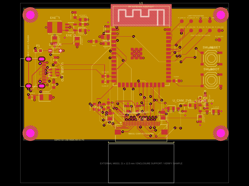 Similar package0hmX/esp32-s3-usb-webcam-ov2640This code defines and integrates a variety of surface-mount, through-hole, and connector hardware components (including microcontrollers, regulators, resistors, capacitors, and connectors) into a PCB design framework, enabling schematic symbol creation, footprint definition, and automated routing within an electronic circuit layout.
 Discover something newastra-abse/t113-s3Allwinner T113-S3 fanout from JLCPCB C5197687: 128 verified escapes, LCD top, storage right; reusable T113S3Module with clean DRC and shorts checks.